3D-Printed Electronics Get Real
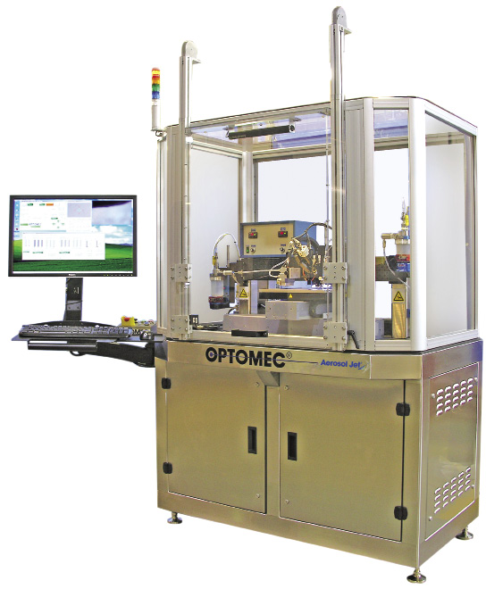
The Optomec Aerosol Jet 3D printing system is capable of depositing materials freely on non-planar surfaces. The system can print traces as small as 10 microns wide, using various conductive nano-particle inks as well as non-metallic conductors, carbon-based resistor inks, dielectric adhesives, semi-conductive inks and more. Image courtesy Optomec.


Latest News
March 1, 2015
Cool, amazing, useful or fun. Any one of these words may describe 3D-printed parts, but the conversation usually centers on end-parts with structural functions—not electrical. Or so you may think. Turns out the first commercially available 3D-printing system for electrical applications came out more than a decade ago and creative work has been escalating ever since.
But what defines 3D-printed electronics, as opposed to standard printed electronics? Does it refer to the materials, i.e., printing layers of electrically conductive plastic? Is it a process that can deposit silver traces alongside plastic in a single build cycle? Or are we talking about generating printed circuitry that conforms to 3D-surface topology, eliminating the need for separate printed-circuit boards (PCBs)? The answer is all of the above and more as new approaches crop up, suitable for applications both exotic and mundane.
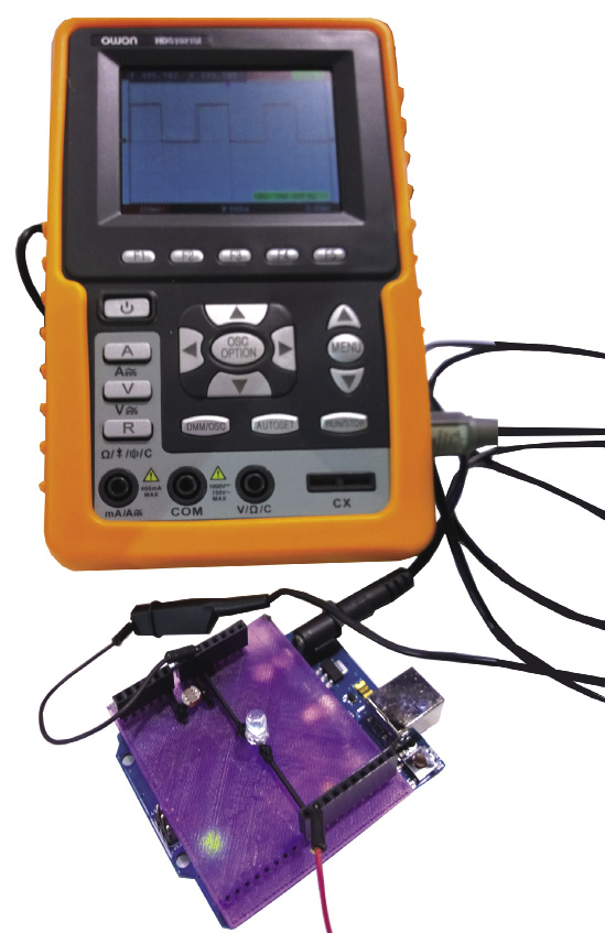 Light-sensor shield board (violet) attached to an Arduino microprocessor motherboard, with photo-sensor and LED connected by electrically conductive, 3D-printed F-Electric filament traces. Image courtesy Functionalize.
Benefits Now and Down the Road
Why might you want to apply 3D printing concepts to electronic circuits in the first place? A little perspective comes from TNO, an independent research organization based in the Netherlands. The group discussed additive manufacturing (AM) opportunities for electronics during the 3D Printing Electronics Conference, held in the Netherlands in January.
TNO points out that most electronics built today require environmentally unfriendly chemical processes to produce PCBs as well as multiple assembly steps to add discrete components. What if, instead, you could print circuits directly on a part, wrapping around it and completely eliminating a separate PCB, or even print an actual electronic component? Such capabilities will simplify today’s electronics manufacturing and create totally new product solutions.
Pioneering 3D-Printed Electronics
If you start a Web search on 3D-printed electronics, you might find all roads seem to lead to Optomec. Though other groups and companies are working on relevant projects, Optomec, a 60-person New Mexico-based manufacturer, has more than 15 years of experience dedicated to this field. Known for its LENS powder-metal AM fabrication systems, Optomec is also the developer of Aerosol Jet technology, a process that creates electronic circuits and components on non-planar 3D geometry. Starting its program in 1999 under the DARPA Mesoscale Integrated Conformal Electronics initiative, the company now has 120 installed Aerosol Jet systems worldwide and works with customers on proof-of-concept efforts at its Minnesota Advanced Applications Laboratory.
 The Optomec Aerosol Jet 3D printing system is capable of depositing materials freely on non-planar surfaces. The system can print traces as small as 10 microns wide, using various conductive nano-particle inks as well as non-metallic conductors, carbon-based resistor inks, dielectric adhesives, semi-conductive inks and more. Image courtesy Optomec.
There are four elements the company says are critical to making 3D-printed electronic technology a success. “With both our LENS and Aerosol Jet technology, we can certainly build a full end-product from scratch,” says Ken Vartanian, vice president of marketing, Optomec. “But in addition, we can add material to an existing structure, which is very different from most 3D printing capabilities out there today. This requires the ability to print freely in 3D space in a conformal manner onto parts that were manufactured in some other way. Most 3D printing systems today cannot do this—you have to start with a flat surface.”
The notion of applying printed materials on substrates to create electronics is not new: Current PCB production involves sophisticated forms of inkjet printing with low viscosity ink or screen-printing using high viscosity ink. So, replacing regular ink with functional ink is one approach. However, Aerosol Jet equipment achieves high precision with a different technology. Its systems use a secondary sheath-gas to aerodynamically focus a primary stream of atomized material and deposit it on non-planar surfaces, creating features as small as 10 microns wide. After low temperature (<200°C) sintering, the traces are fully conductive.
Vartanian lists requirement number two for 3D printing electronics: “When you want to move into high-volume production, the technology needs to be scalable and address various points of the product lifecycle, so you don’t have to go through another process development stage. Change has got to be compelling from a cost and functional stand-point—it can’t just be cool.”
The third factor concerns the big picture of manufacturing. “We don’t quite subscribe to the ‘disruptive technology’ notion of 3D printing,” says Vartanian, “where factories will be a thing of the past. We look to see where we can add value to an existing manufacturing operation; the architecture must be open enough for 3D printing to integrate with existing processes and machines.”
Vartanian notes that a successful open approach also requires working with a variety of low-cost materials available from multiple sources. “We don’t sell materials but we certify them and provide customers with direct access to suppliers,” he says. Aerosol Jet systems print with a wide range of commercial and custom formulations, including conductive nanoparticle inks (with metals such as silver, gold and copper suspended in solvents), non-metallic conductors (carbon nanotubes and conductive polymers), carbon-based resistor inks, dielectric adhesives, semi-conductive inks and even biologic materials.
Customer applications range from cellphone integral-antenna printing by three worldwide contract manufacturers, to thin film transistor (TFT) work done by the University of Massachusetts at Lowell and the University of Minnesota, to a breakthrough alternative to wire-bonding and through-silicon-via (TSV) operations in semiconductor packaging. The latter approach involves printing conformal interconnects directly up a 3D die-stack, with no risk of wires shorting or crosstalk. Aerosol Jet technology is also modular and scalable, supporting multiple print heads in a single system; Neotech AMT in Germany added a four-print-head version to its standard 5-axis CNC (computer numerically controlled) system, creating the AJ 45X, a material handling and deposition system that fits directly into existing manufacturing lines.
Functional Plastics, Functional Inks
An impressive aspect of the 3D printing industry is that it supports activity across a spectrum of organizations, from university research groups to grass-roots inventors to crowd-funded startups. Some projects’ goals are to lay down conductive traces a millimeter or two wide; others are aimed at proving the concept of printing multiple materials for conduction, insulation and connectivity.
Two academic examples that exemplify this are flexible embedded sensors and functional LEDs. The sensor work was begun several years ago by Simon Leigh at the University of Warwick in England. His group used a multi-head Bits from Bytes BFB3000 fused filament system to print a PLA (polylactic acid) glove with embedded motion-sensing strips along the fingers. These strips, formed from a carbon black filled-polyester termed carbomorph, are piezoresistive; even a 0.25 square-micron cross-section was sensitive enough to detect finger-bending.
At Princeton University, Michael McAlpine, assistant professor of Mechanical Engineering, directed graduate students on a proof-of-concept project that 3D-printed a five-layer LED on a hard contact lens. (See “Princeton Combines Plastics and QLEDs in Prototype Contact Lens”) The group modified a pick-and-place machine to deliver quantum LED dots (cadmium selenide nanoparticles coated with zinc sulfide) suspended in a mixture of toluene and dichlorobenzene. The system also deposited layers of four other materials, creating cathode, anode and connector functions in one run.
Controlling the nanoparticle fluid placement across a 2mm-diameter over a curved surface meant finely balancing surface tension vs. nozzle leakage. Using different sized dots created either orange or green LEDs, but at that scale, size difference required a tricky system recalibration. Bringing such technology into manufacturing would involve additional steps such as sintering for full conductivity; acceptable throughput times could be problematic.
“Time is a huge challenge,” says McAlpine. “People can’t figure out what’s the killer app yet for 3D printing, which is still a serial process compared to microfabrication. There’s probably some niche application—printing custom electronics on custom pieces on non-flat surfaces, maybe biomedical devices—some next-generation application that no one is yet sure of where slow throughput matters less than the need for customization.”
Supplying the Filament World
In the past few years, the thought of creating conductive filament materials that bypass the need for PCBs has also appealed to creative private businesses. Such filaments combine plastic with embedded particles that allow 3D-printed parts to display electrically conductive properties. The printed-feature size does not compete with the industrial capabilities of Optomec systems, but the materials give new functionality to open-source equipment and are improving month by month.MakerGeeks markets a 1.75mm-diameter conductive filament that is ABS (acrylonitrile butadiene styrene) based and contains a blend of carbon fiber and carbon black particles, with a stated resistivity range of 10,000 to 12,000 ohm-cm (See “Resistance, Resistivity and Surface Resistance” sidebar); price is $23/lb. Online comments indicate if users are careful to print at low speed to avoid filament breakage, the material is useful for making an electronics case with an integrated ground. Because resistivity needs to be at least a thousand times smaller for behavior closer to that of metals, it’s no wonder a lot more work is underway by a number of entrepreneurs.
Though little more than a year old, ProtoPlant now manufactures six types of (in their words) exotic filaments. The company recently announced funding of its second Kickstarter project, supporting the new Proto-pasta Conductive PLA. The material is a compound of conductive black, a dispersant and PLA, and is sold in both 1.75mm and 2.85mm versions. The volume resistivity of molded resin (not 3D printed) is 15 ohm-cm; for example, resistance of a 10cm length of 1.75mm filament is 1.8 Kohm. Conductivity is suitable for such applications as touch-sensor projects and simple circuits. Expected pricing: $48/500g spool ($43.50/lb).
Functionalize is another new materials company born out of the desire to readily 3D print circuitry. President and founder Mike Toutonghi, in looking for ways to assemble electronics without soldering, drew on his early interest in chemistry to set up his own nanotechnology lab. Several years of work led him to synthesize a conductive compound of PLA, carbon nanotubes and metal composite that displays resistivity of <1 ohm-cm. The company is now marketing its F-Electric PLA filament through ProtoParadigm, a manufacturer of basic, colored and specialty filaments.
Toutonghi says although F-Electric’s pricing is about $140/lb, the filament’s use can be validated when used as a small percentage of a 3D-printed part, with the majority of the part built from standard PLA for structural integrity. He’s working on lower-cost formulations but is also exploring another intriguing property of the material, its signal frequency bandwidth of about 200 MHz. “This could be a challenge,” he says, “but it’s close to the ability to put gigabit/second data on it.”
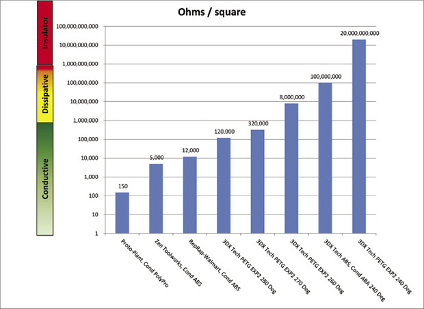 Comparison of surface resistance values [ohms/unit square] for several conductive 3D printing materials. Image courtesy ProtoPlant.
More Developments, More Directions
News related to printing conductive materials is now an almost daily event. AutoX3D, maker of industrial-grade personal printers, just announced a water-cooled extruder system that may address the nozzle clogging that can happen with conductive (filled) filaments. And a filament printhead add-on from RabbitProto will let users deposit conductive silver ink (Electric Paint) supplied by Bare Conductive; trace width is 0.84 inches from standard nozzles and surface resistivity is 55 ohms/square for 50-micron thick deposition.
Working on yet another inexpensive way to bypass traditional PCBs (even printing on fabric), Australia-based Cartesian obtained Kickstarter funding to develop the Argentum open-source 3D printer. The Argentum employs dual inkjet cartridges to lay down two-part material: the first deposits a silver-nanoparticle solution then the second retraces the same CAD-directed pattern with simple ascorbic acid. The two liquids combine to create a silver precipitate, which dries into conductive traces determined by nozzle size. Systems began shipping last summer; the site says batch four will ship this month.
Lastly, the 2015 International Consumer Electronics Show saw the debut of the Voxel8 dual material two-nozzle 3D printer from Voxel8 of Somerville, MA. Founded by Dr. Jennifer Lewis, Wyss Professor of Biologically Inspired Engineering at Harvard University, the company is based on more than a decade of university work. The system trades off depositing PLA filament with pneumatically dispensed conductive silver ink during a single build, supporting creation of embedded conductors, wires and batteries. Nozzle size for the silver is 250 microns; material resistivity is 5.0 x 10⁻⁵ ohm-cm, and other materials are coming. Voxel8 has worked with Autodesk to develop Project Wire software that lets users create a 3D mechanical design with embedded conductive traces for printing on the Voxel8 system.
More Info
Subscribe to our FREE magazine, FREE email newsletters or both!
Latest News
About the Author
Pamela Waterman worked as Digital Engineering’s contributing editor for two decades. Contact her via .(JavaScript must be enabled to view this email address).
Follow DE

