
The rise of the IoT brings with it a cornucopia of applications and disparate design requirements. This has triggered the development of greater chip-configuration diversity. As the IoT takes shape, a new hardware era will emerge, where design engineers will harness the power of all options to meet expanding demands for new functionality. Image courtesy of Optimal Design.


Latest News
November 1, 2017
For the past 10 years, smartphone technology has been the primary driver of innovation in the electronics industry, because chipmakers have constantly pushed to produce smaller, denser, cheaper and more powerful electronic components. To accomplish this, PC and smartphone designers have leveraged system-on-a-chip (SoC) technology. This IC (integrated circuit) model greatly facilitates integration—addressing space constraints—and enables economies of scale by fabricating the same chip designs on common process platforms in production runs of millions of units. During this period, the advantages of cost and integration outweighed any of the SoC’s shortcomings.
But this dynamic seems to be changing. Smartphone technology’s footprint in the market has begun to shrink and, at the same time, internet of things (IoT) technology has taken on a more dynamic role. Research firm MarketsAndMarkets predicts that the global IoT market will grow to $561 billion by 2022, sustaining a compound annual growth rate of 26.9%.
 The rise of the IoT brings with it a cornucopia of applications and disparate design requirements. This has triggered the development of greater chip-configuration diversity. As the IoT takes shape, a new hardware era will emerge, where design engineers will harness the power of all options to meet expanding demands for new functionality. Image courtesy of Optimal Design.
In addition to changing market dynamics, the rise of the IoT also portends a fundamental shift in the hardware building blocks used by design engineers to develop products. But why are these changes occurring now? After all, PC and smartphone designers have long been integrating increasingly complex combinations of processing, communications and sensing components, pushing the limits of form, size, power consumption and functionality. What does this paradigm shift mean for design engineers? And what hardware building blocks will dominate the products they produce for the IoT?
Catalysts for Change
The trigger for this shift lies in the fact that the design and market requirements of the smartphone and the IoT differ greatly. With the rise of the IoT, there is no longer a single semiconductor fabrication process that works for all of the components incorporated in a system. This runs counter to the parameters of SoC production, where these systems are locked into a single production process that essentially precludes using best-in-class components to build the systems. This means that one or more essential components must be compromised. The only way to implement the kind of customization required by the diversity of IoT applications is by reconfiguring the entire SoC fabrication line, which would greatly diminish one of its primary strengths—the fab’s ability to deliver economies of scale.
The rise of the IoT, with its breadth of applications and disparate design requirements, is forcing product designers to seek greater chip-configuration diversity. And instead of being able to use the same chip design for millions of applications, the IoT places a higher value on customization of products manufactured in moderate-size production runs.
 SoCs greatly facilitate integration by placing digital, analog, mixed-signal and RF subsystems on a single substrate. This IC model addresses space constraints and promises to speed development. But because all these elements are placed on the chip via a common manufacturing process, it is difficult to implement customization without compromising the approach’s ability to leverage economies of scale. Image courtesy of Silicon Labs.
As a result of these shifting dynamics, chip makers have adopted different approaches to IC and component packaging and have begun to generate new chip designs. A major trend called system-in-package (SiP) combines one or more ICs of different functionality in a single package that performs as a system or subsystem.
The question then becomes: What chip models and configurations will become the building blocks of the IoT, and what roles will each of the variations play in the creation of new products? Will one approach dominate, or will the industry use a combination of approaches? And how will this affect product development teams? The answers to these questions become clearer after an examination of the strengths and weaknesses of each approach.
SoCs, SiPs and Other Options
SoCs and SiPs each bring strengths and weaknesses to the table. It’s important, however, that designers bear in mind that there are other options that may serve them well.
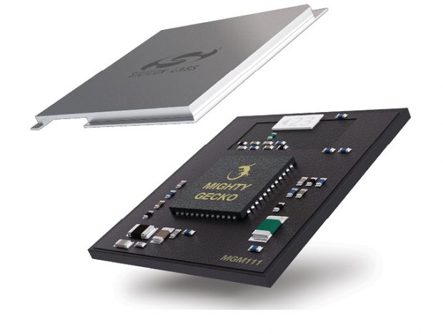
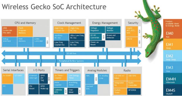 Silicon Labs’ wireless Gecko system-on-chip (SoC) integrates an ARM Cortex-M4 core; 2.4 GHz radio and hardware cryptography. One of the SoC’s greatest strengths is the wireless technology incorporated in the system, which includes Thread and ZigBee stacks for mesh networks, radio interface software for proprietary protocols, Bluetooth Smart for point-to-point connectivity and Simplicity Studio tools to simplify wireless development, configuration, debugging and low-energy design. Image courtesy of Silicon Labs.
Looking at SoCs, economies of scale represent one of their greatest strengths, but there are other positive elements to consider. For example, they offer the smallest footprint and often provide the lowest power implementation.
Their drawbacks, however, are significant. “SoCs present serious development risks, such as mask errors and firmware bugs,” says Todd Zielinski, senior director of electrical engineering at the Bresslergroup, a Philadelphia-based design firm. “They can also be difficult for novices to use and may be difficult to access because of minimal design support from manufacturers.”
But when sizing up this chip model, engineers must also consider the technology against the backdrop of wireless design issues. “For companies with in-house RF (radio frequency) expertise and experience developing RF products, reusing R&D investments and designs based on SoCs often makes these devices a better approach,” says Kamran Shah, director of corporate marketing at Silicon Labs. “Also, for any proprietary wireless design with unique antenna and other RF design needs, an SoC will generally be preferable.”
Compared with these strengths and weaknesses, SiPs offer an interesting contrast. For example, SiPs often provide more capabilities for less volume of parts shipped than SoCs. This chip model also “is more accessible to the lower volume developer through normal sales channels, and has less risks in development—[because] they are usually built from a composite of well known and available parts in die form,” says Zielinski. “They have slightly higher costs in production than SoCs, but [that] can be offset in development costs in lower volumes.”
Designers should also be aware that SiPs are easier to customize for less money than SoCs. This directly relates to the manufacturing constraints posed by the fact that SoCs are locked into a single production process.
Considered within the context of wireless design challenges, SiP strengths can be stated by a few rules of thumb. “For wireless systems, the selection of an SoC or certified SiP module tends to come down to expected volume, time to market and in-house RF expertise,” says Shah. “For fast time-to-market requirements, certified SiP modules have a significant advantage as they reduce both cost and time for regulatory certification. For companies without in-house RF expertise, certified SiP modules are also a much lower risk to embark on a project as the complexities of antenna design, PCB (printed circuit board) layout and RF testing and verification are addressed already.”
After looking at the strength and weaknesses of the two technologies, it’s clear that design engineers have their hands full, weighing all the considerations and tradeoffs involved. And to make matters even more complicated, there are also cases when an SoC and an SiP module can both be used in a design. For instance, a development team could use a certified SiP module as a network co-processor device for wireless communication with an SoC.
But just how big a role can either of these technologies play in IoT product development? Is reliance on pre-built, plug-and-play SoCs and SiPs that incorporate prepackaged sensor, mixed-signal, signal processing and wireless subsystems a viable design approach?
The Plug-and-Play Option
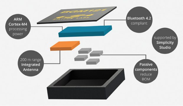 Silicon Labs’ Blue Gecko BGM12x Bluetooth Smart SiP integrates a Bluetooth 4.2-compliant stack capable of running end-user applications onboard, as well as 256 KB of flash memory and 32 KB of RAM. The entire package measures 6.5x6.5x1.4 mm, making it well suited for space-constrained applications. Image courtesy of Silicon Labs.
The use of drop-in, prebuilt SoCs or certified SiP modules can be an ideal way for development teams to incorporate functionality quickly into designs. For most standards-based functionality, relying on commercial solutions can sometimes simplify the design process and speed development. But here’s the catch: Prebuilt modules can save time, but they often increase unit cost as much as two-fold. They also limit flexibility in packaging, features and environmental constraints. The SoC-based approach also requires in-house RF expertise to ensure performance and integration requirements are met, and not all companies have these resources. Development teams adopting the SoC-based approach must address factors such as antenna design, PCB layout, component interactions, RF test equipment and worldwide regulatory approval.
Long term, for the IoT, an approach that relies solely on drop-in, prebuilt modules promises to fall short. “We need to remember that the IoT is not one application but a set of hundreds, if not thousands, of different applications,” says Ron Lowman, strategic marketing manager for IoT at Synopsys. “So there is a broad range of differing specs required for the analog and RF components of these systems. This reduces the volumes and thus the potential profitability of embedding the specific RF and analog IP based on development costs. Also, the strategy to use plug-and-play SoCs or SiPs in IoT devices up to now has worked only because of these profitability hurdles.”
To address this hurdle, Lowman says companies have sought to reduce their investment and maximize their capacity to get product to market faster. They do this via leveraging SiPs and plug-and-play prepackaged alternatives instead of analog and RF integration.
So for development teams, the decision to use a certified SiP module or an SoC comes down to expected volume, time-to-market requirements, aggressive design and RF requirements and available in-house expertise. Based on these conditions, it seems unlikely that developers will be able to rely solely on drop-in, prebuilt SoC and SiP modules, although they will definitely be part of the mix.
This raises the question: When would design teams be best served by specifying and combining individual subsystems (for example, microcontroller unit, memory, RF module) rather than relying on plug-and-play systems like SoCs or SiPs to handle the integration?
Building Your Own
The viability of custom development is greater for products that are expected to be in very high volume or have extremely complex and unique requirements for a market. “In the case of very high volumes, the potential cost savings in hardware with an optimized solution might outweigh the expense of hardware or RF expertise, additional test infrastructure and wireless certification,” says Shah. “In the case of complex systems that may not be able to make use of standards-based technology, the only technical option may be a more custom implementation, where an SoC or certified SiP module may not meet all of the design requirements.”
Specific technical challenges mandate custom development, such as when a systems form factor requires additional flexibility, as pointed out by Joe Kreidler, director of electrical and software engineering at Optimal Design, an Illinois-based product development and IoT solutions firm. “Optimal Design has found this [custom development] to be particularly the case with wearables. Even though a module may be a simpler solution from a board design and firmware perspective, a module may not be able to bend or be shaped around the curve of the body. In these cases, utilizing discrete components allows us to lay out the electronics to obtain the optimal size and shape necessary for the desired user experience.”
Another instance where development teams are best served by custom development involves designs with tight power budgets. “In battery-operated devices, it’s required that the subsystem be integrated to ensure extended battery life and cost reductions,” says Lowman. “In a study by Microsoft, one of the largest differences from chip-to-chip power consumption comparisons was the length of time required to turn on the processor and turn off the processor. Integrating the wireless and analog components and sticking them on the AHB (advanced high performance bus) can save five to six cycles versus a serial interface connected to the plug-and-play systems.”
Additional benefits include the increased time to turn on and off a second processor and second power management piece that may be on the external SoC/SiP, Lowman adds.
When is Expertise Required?
Even before development teams begin to consider what hardware building blocks to use in their IoT product design and whether to pursue a custom implementation, they have to determine if they have the right balance of expertise to carry out the project. With the complexity of the designs, ever-increasing incorporation of analog and RF subsystems, and the array of hardware components engineers have to choose from, having the necessary talent represents a critical factor.
A good rule of thumb states that the level of analog and RF expertise needed for a design project is largely a function of the type of product being delivered, the wireless communication protocol used and the level of integration of sensors and peripherals required. “A project relying on a standards-based wireless protocol, such as Bluetooth, can make use of certified modules and standardized protocol software without the need for extensive RF or analog design expertise,” says Shah. “On the other hand, a company developing a proprietary wireless protocol may require optimization to meet system requirements in both software, hardware and antenna design.”
Add the integration of wireless to a project developing a wearable, and the need for RF expertise grows. In this case, engineers typically do not have the luxury of using drop-in modules. Discrete components may be needed, and the device generally requires a custom antenna to meet size and performance requirements. For these devices, in-house RF expertise is essential to the success of the product.
“To build a successful product with embedded radios, RF simulation is needed from the beginning of the project,” says Pete Nanni, lead RF engineer at Optimal Design. “The complete RF system consists of the module, printed circuit board and housing. An engineer cannot simply use data sheet performance specifications and radiation patterns because these patterns are measured in free space.
“When a module is built into a system, the radiation pattern changes, so simulation is key to optimizing RF performance. Many IoT devices have multiple radios, such as a Bluetooth Low Energy radio and a cellular radio,” Nanni adds. “Off-the-shelf modules can be used, but the reference designs do not provide information about the interaction of the modules. An in-house RF team needs to perform simulations to understand how the radiation patterns are impacted by the multiple radios.”
Challenges of a New Hardware Era
The hardware options of engineers designing products for the IoT have increased, facilitating the integration of digital, analog, mixed-signal and RF functions, and sometimes streamlining the development processes. But even with these building blocks in place, custom implementations will still be required in the most demanding of designs.
No single chip design will dominate development processes. In fact, designers will sometimes combine SoCs, SiPs and other multichip modules in a design. The decision to use a certified SiP module or an SoC will often come down to expected volume, time-to-market requirements, aggressive design and RF requirements, and available in-house expertise.
Expanded use of analog, mixed-signal and RF subsystems will place a premium on in-house expertise. Development teams with this expertise will have a greater opportunity to take advantage of the full spectrum of hardware options available to them, allowing them to better meet demands for smaller form factors, greater energy efficiency and enhanced functionality.
Subscribe to our FREE magazine, FREE email newsletters or both!
Latest News


