Electroninks Makes Metal Conductive Inks
Inks cut need for traditional deposition methods and are eco-friendly.
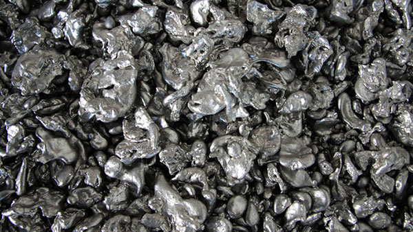
Electroninks offers silver, gold and platinum-based inks in their MOD platform, with others (including nickel and copper in prototyping phase).


April 28, 2022
Electroninks, Inc., makes available its full suite of metal organic decomposition (MOD) conductive metal ink solutions. Electroninks offers a line of ink products, including a small (desktop) prototype additive manufacturing solution for rapid on-demand printed circuit board (PCB) printing and repair, called CircuitJet.
Based on Electroninks metal-complex chemistries, these materials are referred to as “particle-free” inks due to their translucent nature. This chemistry, inspired by precursors used in vacuum deposition techniques and now built into printed inks, provides product designers and manufacturers of most hardware devices a new palette of electronic materials for printing performance circuitry.
Electroninks operates out of a new 30,000-square-foot R&D and production facility in Austin, TX. The company is a key supplier for the U.S. Department of Defense (DoD), including the U.S. Air Force.
“Traditional conductive inks and metal deposition methods have been around for decades, but are slow, problematic, expensive, and not at all environmentally friendly,” says Brett Walker, co-founder and CEO, Electroninks. “Our metal complex particle-free inks radically change the game. They’re our secret sauce and set a new standard for conductive inks in 21st century electronics manufacturing.”
Electroninks offers silver, gold and platinum-based inks in their MOD platform, with others (including nickel and copper in prototyping phase). These ink technologies generally fall into three product lines:
CircuitShield: Low maintenance ink products for EMI Shielding and back-end semiconductor metallization. CircuitShield powers the technology that produces smartphones with 5G capabilities. CircuitShield eliminates spray nozzle clogging, residue in silver film and provides high shielding effectiveness. With long shelf-life and printing stability at room conditions. It is used for 5-sided SiP shielding with aspect ratio from the top to the side wall close to 1. Other use-cases involve wafer metallization and conformal via coating.
CircuitWrap: Ink products used as bezel/wrap electrodes in touch panel displays, and micro/miniLED panels. With electrical and mechanical performance in a <2um thickness film, CircuitWrap is considered an ideal material for bezel electrodes in touch panel (and foldable touch panels), wrap electrodes in micro/miniLED panels, and metal mesh films for flexible display technologies. Electroninks’ particle-free ink technology allows for deposition onto patterned substrates that will be metallized to create a fine metal mesh. Panel-makers and OEMs in OLED, micro/miniLED can produce foldable touch-screens for displays ranging in size from sets, to mobile, to AR/VR lenses.
CircuitSeed: Thin, dense films used as 3D/finely patterned seed layers for subsequent metallization by plating. A more efficient method for plating electronics, it supports multiple chemistries that can be printed via various techniques as dense, finely patterned seed layers on surfaces ranging from rigid to flexible plastics, and even 3D.
Rapid On-Demand PCB Prototyping
Electroninks has a small (desktop) prototype additive manufacturing solution for rapid on-demand PCB printing and repair, called CircuitJet. CircuitJet enables customers that need fast PCB prototyping on up to an 8x10 form factor with an “all-in-one” tool that retails for under $5,000 USD.
Designed for Manufacturing
CircuitJet, CircuitSeed, CircuitShield and CircuitWrap cut the need for traditional deposition methods while simultaneously enhancing the production of applications that require materials at lower costs. From electronic and mobile displays, rigid PCBs and medical devices to electromagnetic shielding and e-textiles, Electroninks’ solutions are targeted for a range of manufacturers.
The traditional subtractive design and manufacturing process uses more material that generates more waste, adding to environmental challenges. Electroninks’ solutions are additive: they use 3D printing technology to add layer upon layer of metal ink to create miniaturized circuitry.
All products are available for immediate use in high-volume, production scale applications, and can also be customized.
Sources: Press materials received from the company and additional information gleaned from the company’s website.
Subscribe to our FREE magazine, FREE email newsletters or both!
About the Author
DE’s editors contribute news and new product announcements to Digital Engineering.
Press releases may be sent to them via [email protected].


