Making Flexible Hybrid Electronics a Reality
October 1, 2017
 Tom Kevan
Traditional sensing systems just aren’t cutting it these days. Rigid and fragile, they simply cannot support some of the wearable and Internet of Things applications that the medical, consumer electronics and military sectors are demanding. To address this issue, electronics manufacturers have turned to printed electronics, but even here, shortcomings hinder progress.
Although this technology has advanced quickly, manufacturers have been able to mass-produce only sensors with simple structures, such as disposable blood glucose sensors. What the market needs are more complex, flexible systems that sense, process and communicate; therein lies the rub. Mass-producing complex printed sensing systems that include processing and communications modules requires designs that incorporate printed and advanced CMOS-based (complementary metal–oxide–semiconductor) components, and until recently, no one in the industry has developed manufacturing processes that can produce such systems.
This may be about to change. Companies, research facilities and government agencies have ramped up efforts to develop production infrastructures that can cost-effectively mass-produce a new generation of electronic devices called flexible hybrid electronics (FHE). By harnessing printed and advanced CMOS-based components, manufacturers will be able to deploy systems on substrates that can conform to organic shapes and stretch while delivering advanced functions.
Hurdles
When manufacturers have tried to develop advanced flexible electronics that incorporate CMOS-based components and printed electronics, they have been foiled by the limitations of current silicon technology. Traditional chips measure between 100 microns and 300 microns in thickness. Unfortunately, these are brittle, crack when bent and cannot conform to curved surfaces. Recent research, however, has shown that manufacturers can produce flexible chips by reducing the die’s thickness to less than 50 microns.
The problem has been that chipmakers do not have the means to create, place and interconnect thin die. Today’s fabrication plants rely on pick-and-place methods using automated robotic equipment to attach integrated circuits (ICs) to substrates, picking up individual chips from a wafer and placing them at predetermined attachment points. But when fabs have reduced the size or thickness of ICs to improve flexibility, pick-and-place techniques fail.
A New Production Paradigm
One company taking on the manufacturing challenges facing FHE is Uniqarta. The Cambridge, MA-based startup has developed a manufacturing process that could open the door for embedding ultra-thin ICs in flexible substrates, such as paper.
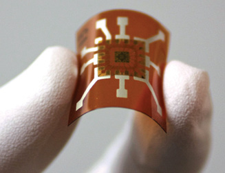 Flexible hybrid electronics could help overcome the physical limitations of silicon IC obstacles. Images courtesy of Uniqarta.
The process, called FlexChip, consists of tailored assembly steps that perform thinning, dicing, placement and interconnection, promising to transform commercial off-the-shelf die into ultra-thin ICs. Key to this process is the “handle wafer,” a support wafer bonded to the device IC. The material preparation step bonds this support material to commercial off-the-shelf wafers. This allows wafers to be thinned to the desired thickness and then diced without compromising the physical integrity of the device IC.
Each die/handle combination has a thickness comparable to a standard die. As a result, it can be handled and positioned using standard die bonder equipment. A die bonder then flip-chip assembles each die/handle onto a substrate. Because it is bonded to the die with a heat-sensitive adhesive, the handle wafer is released during the thermal cure cycle, when the die is bonded to the substrate. The handle is then removed, leaving behind only the ultra-thin die. FlexChip can be used with any type of semiconductor wafer or die without any modification to the semiconductor fabrication process.
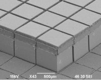 Uniqarta has developed an ultra-thin chip fabrication process called FlexChip that could provide manufacturers with the means to cost-effectively mass-produce flexible hybrid electronics. A support structure called a “handle wafer” allows the production of chips with thicknesses of less than 50 microns, guaranteeing structural integrity in the process. The image here shows the various stages of IC assembly with and without the handle wafer.
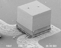 (At left): Post-dicing, with die/handle stack; (above): Ultra-thin die/handle stack.
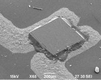 (Above): Ultra-thin die after the handle has been removed.
FlexChip supports two die placement methods: pick-and-place or laser transfer. Pick-and-place is most suitable for use with assemblies that are sparsely populated or involve ICs of different types or with processes using existing equipment. The laser transfer method is tailored for high-speed assembly lines with closely spaced identical ICs, such as with RFID (radio frequency identification) inlays. Uniqarta contends that the laser transfer method can achieve placement rates in excess of 100 million units per hour in high-density applications.
Moving Forward
Companies like Uniqarta have moved FHE closer to becoming a commercial reality. The emerging class of flexible hybrids promises to enable manufacturers to create sensing systems that conform to organic shapes, flex with natural body movements and incorporate processing and communications components.
This translates into the introduction of applications that extend the reach of sensors. Wearable and conformable architectures will allow design engineers to embed sensing systems on or in civil structures, automobiles and aircraft, with an eye on monitoring structural integrity. FHE also promises to revolutionize wearable devices that monitor vital signs to optimize healthcare and even allow medical professionals to deploy biomarkers to monitor chronic conditions.
Subscribe to our FREE magazine, FREE email newsletters or both!


