Nanoscale 3D Printing Material Targets Microelectronics Applications
Stanford researchers marry metal nanoclusters with common polymers to create better lightweight 3D printed protective lattices.
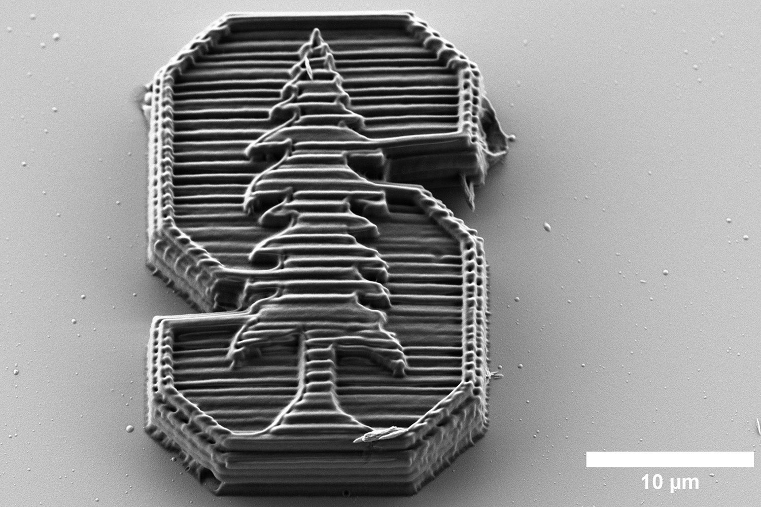
Nanoscale 3D printed material, with energy absorption strengths, is a strong candidate for lightweight protective lattice structures for microelectronics gear. Image Courtesy of John Kulikowski


March 1, 2023
Satellites, drones, and microelectronics—all critical innovations with a lot of complex circuitry and technology that needs structural protection, just at a very small scale.
A team of researchers at Stanford University has come up with a solution for creating optimized, lightweight protective lattices for these structures built around nanoscale 3D printing. Their development is a new material designed for 3D printing at the nanoscale, which means the tiny lattice structures are sized at a fraction of the width of a human hair, making them lightweight and strong enough to handle the specific requirements of these applications.
To create the new material, the researchers took their cues from nature, specifically bone, which drives resiliency from the combination of a hard exterior, nanoscale porosity, and small amounts of soft material. Marrying a 3D structure with multiple, well-designed materials allows bones to transfer energy with minimal opportunity for breakage even though they remain relatively lightweight.
This design sensibility drove the Stanford research team on its new material design journey. The resulting material, able to absorb two times the energy of other 3D printed materials of similar density, draws some of its power by incorporating metal nanoclusters (essentially small clusters of atoms) into common classes of polymers such as acrylates, epoxies, and proteins that are routinely used in 3D printing. This recipe combination also accelerated the rate of printing to 100 millimeters per second—approximately 100 times faster than what has been previously achieved in nanoscale protein printing.
The research team is 3D printing the materials using a two-photon lithography method, which hardens printing materials through a chemical reaction set off by laser light. They see the 3D material as a good candidate to provide improved lightweight protection for fragile pieces of equipment found in satellites, drones, and microelectronics.
Wendy Gu, a mechanical engineer at Stanford and one of the authors of a paper in Science magazine describing the material and process, said there’s a lot of interest in the design of 3D structures that can bolster mechanical performance. The team tested the new material with multiple lattice structure configurations, with some instances focused on carrying a heavy load and others aimed at absorbing impact. The metal nanocluster-polymer composite and the 3D printing process delivered an optimal mix of energy absorption, strength, and recoverability, Gu said.
“What we’ve done on top of that is develop a material that is good at resisting forces,” she said, in a prepared release. “It’s not just the 3D structure, but also the material that provides good protection.”
The Stanford research was supported through grants from the U.S. National Science Foundation (NSF) and through NSF support for the Stanford Site of the National Nanotechnology Coordinated Infrastructure.
This video explains how nanoscale 3D printing can enable advanced manufacturing for certain classes of products.
Subscribe to our FREE magazine, FREE email newsletters or both!
About the Author
Beth Stackpole is a contributing editor to Digital Engineering. Send e-mail about this article to [email protected].
Follow DE

