Nanotechnology Enables Real Atomic Precision
From the bottom up or the top down: nanotechnology garners $1.6 billion of the President's 2010 budget.


Latest News
October 1, 2009
By Susan Smith
While nanotechology might mean different things to different people, the term was originally coined to describe the building of things from the bottom up with atomic precision. That, says Steve Vetter, CEO of Molecular Manufacturing Enterprises of Saint Paul, MN, means “a place for every atom and every atom in its place.”
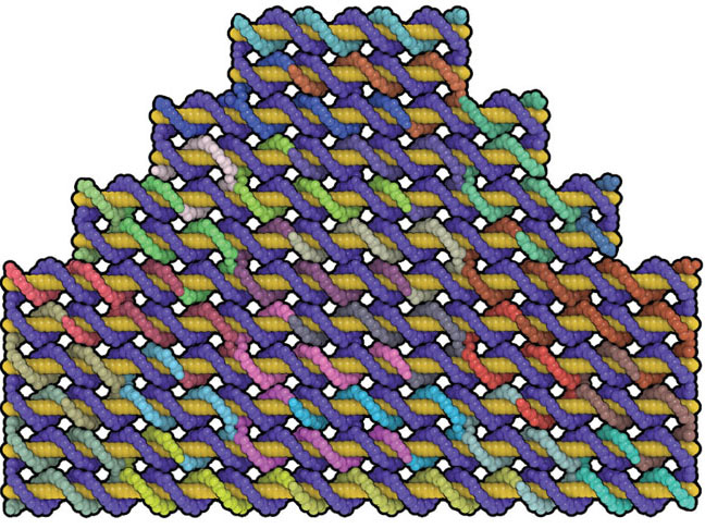 This model, titled DNA origami, was modeled using NanoEngineer-1, which includes special support for DNA structure design. It represents a milestone in the field of nanotech due to the affordability and simplicity of fabricating billions of DNA nanostructures at one time. In the image above, each strand of DNA is given its own color. Image courtesy Paul Rothemund, CalTech |
Noted physicist Richard Feynman gave a talk at the 1959 meeting of the American Physical Society at the California Institute of Technology (Caltech) entitled, “There’s Plenty of Room at the Bottom,” about designing to the atomic level versus miniaturization. He talked about microscopic biological systems that can manufacture substances and move around on a microscopic scale.
Yes, Manufacture
For almost 20 years Boris Fritz has run rapid prototyping labs at Northrup Grumman. “I began to realize a lot of work done in nanotechnology is actually additive layer fabrication,” he said. “I wanted representation at the Society of Manufacturing Engineers (SME) for nanotechnology because SME focuses on manufacturing.”
Nanotechnologists typically focus more on nanoscience, said Fritz, than on the manufacturing side, yet ultimately nanoscience is headed toward creating useful manufactured products. The scale being investigated is measured in nanometers, a bit more than 20 times the diameter of a hydrogen atom; the average human hair is about 100,000 nanometers in width.
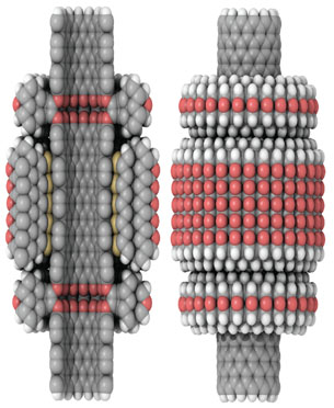 The strength and stiffness of carbon nanotubes have made them important as building materials in many current nanoscience applications. Their range of use is expected to extend to molecular manufacturing applications in nanoscale scaffolding and molecular electronics. Their cylindrical shape and electronic structure make them interesting components in designs of molecular bearing assemblies. Image courtesy Damian G. Allis, dept. of Chemistry, Syracuse University |
To help get us there, the National Nanotechnology Initiative—managed within the framework of the National Science and Technology Council (NSTC)—resolved to coordinate federal nanotech research and development in 2001. Spearheaded by the Foresight Institute (FI), the initiative took a detour, according to Vetter, when members of the Nanotech Business Alliance and “others” shifted the definition of nanotechnology away from “building from the bottom up with precision” to “building anything under 100 nanometers.”
“That’s the current definition you’ll find almost anywhere because there’s almost $1 billion of government money heading towards that definition,” explained Vetter. “The problem is there are a lot of things under 100 nanometers, in fact one of the chip manufacturers said everything we do is under 100 nanometers, so every chip would qualify as nanotechnology, which is crazy. It’s too broad of a definition; it completely siphons off the money that should be going to the atomic precision stuff.”
FI and many of its followers are doing what they can to fix this. According to Vetter, the group hired a consultant in Washington to try to help at one point, but “it is a steep uphill battle…. There has been a tiny bit of progress in the sense that recently a few small DARPA grants have focused on a few key steps leading toward atomically-precise manufacturing.”
The President’s 2010 budget for nanotechnology provides $1.6 billion for the National Nanotechnology Initiative (NNI), which does show commitment and promise for the industry. Currently the NNI involves the nanotechnology activities of 25 federal agencies, 13 of which have budgets for nanotechnology research and development for 2010. Included on the list of participating federal agencies are the Department of Homeland Security and the National Institutes of Health (NIH).
CAD and Nanotechnology
If Feynman’s vision is correct, then how designers scale down CAD capability to design at the nano level and how the process of building from the bottom up is controlled at the nano level becomes the challenge.
Software called NanoEngineer from Nanorex.com, developed by Mark Sims, begins to address the challenge. In this case, the software for nano design is a CAD software. The trick is taking the effects of classical physics in normal scales and reconciling them with the atomic world of quantum mechanics.
According to Tihamer Toth-Fejel, a senior research engineer at General Dynamics of Falls Church, VA, additive rapid technologies might offer some answers. He says there are a number of processes that will be able to do this at the nanoscale; the DARPA-funded Tip-Based Nanofabrication Project, for example, has nine different teams working on developing this technology.
At the nano level, dip-pen nanolithography from NanoInk is used to achieve a layer-by-layer process using atomic force microscopes (AFM) with non-passive tips that interact with atoms.
“It doesn’t just give you an interpretation or visual image, so you have these silicon nitrite tips and diamond tips, where the tip goes from 8 microns down to 15 nanometers—so it’s the world’s smallest pen, 15 nanometers, and there you can have an ink that writes the stuff in the atoms,” said Fritz. “It’s a solvent that holds nanoparticles or DNA so you can interact and deposit things layer by layer. The dip-pen lithographic process will use as many as 55,000 pens in an array with multiple materials to create things at the nano level.” One of the goals, said Fritz, of making integrated circuits at the nano level to produce more powerful computer chips.
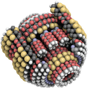 This is the MarkIII(k), a nanoscale planetary gear that couples an input shaft via a sun gear to an output shaft through a set of planet gears. The planet gears roll between the central sun gear and a ring gear on the inner surface of the casing. Image courtesy of K. Eric Drexler , Nanorex, Inc. |
It’s a type of atomic spray painting on surfaces, one layer at a time, using a kind of chemical vapor deposition process. Nearly perfect crystals can be grown, one atomic layer at a time. For example, 70 percent of the world’s supply of solid-state semiconductor lasers used inside of CD players are made this way. “This method can produce a square centimeter of this semiconducting laser that’s over one quadrillion atoms with as few as three atoms out of place.”
Futuristic Nano
Fritz said there are other ways. Chemistry has been doing nanotechnology forever, it turns out, but it has been doing it without precise control. That precise control of only three atoms out of a quadrillion being out of place defines nanotechnology. Chemistry creates a chemical reaction of Avogadro’s numbers of atoms (1023) but comes with no global location control or local orientation control over where each atom goes.
That kind of control is exemplified in the example from Nanorex’s NanoEngineer, which helps design DNA to generate a specific shape (such as billions of DNA smiley faces) which could lead to hundreds of throwaway supercomputers on a fingertip.
Changing the Future
Self-replication is not a new idea; it was a dream of mathematician and philosopher Renee Descartes in the 17th century. Fritz describes the best example of self-replication in nature as fire. “As long as you have the substance to burn and oxygen and heat, the fire will keep on replicating forever. It’s a self-replicating process. At the nano level we could start replicating things, like one desktop nanofactory making a second desktop, like one robot making another robot. But right now a lot of that self-replication is happening in rapid prototyping –so you have places like MatLab at MIT and RepRap and several others talking about this.”
The additive layer allows for full assemblies to be grown layer by layer at the nano level. At Nanorex.com, founder of the Foresight Nanotech Institute, Dr. Eric Drexler, considered the “father of nanotechnology,” has designed a roadmap that shows the building of subassemblies into higher-level assemblies inside a desktop factory, which then manufactures the product of your choice. The ultimate goal is to create a desktop nanofactory appliance that could be used in your home to build anything you need.
DNA and fake blood cells, or “respirocytes,” are also in the works. “If we replace 10 percent of your blood with those respirocytes, then you can hold your breath for four hours,” Fritz said. “That way, if you have a heart attack you can call the hospital and tell them you’re going grocery shopping first and then stop by the hospital and they will have everything ready.”
DNA Origami was invented by Dr. Paul Rothemund, and a practical application has been demonstrated at Arizona State University to help doctors identify pathogens by giving a scraping to the lab on a chip. It can determine which pathogen you’re suffering from just by analyzing its RNA—assuming of course that the one you are suffering from is part of its “library.” Currently, it can only identify three RNA strands, but it does it almost perfectly, even with extremely low concentrations.
Another possibility are “foglets,” micron-size robots made of nanoscale parts that have little arms that hook together. The idea was developed by J. Storrs Hall, author of Nanofuture: What’s Next for Nanotechnology. Foglets are run by a simple software that enables billions of them to act like shapeshifters. A large enough collection could reform into different furniture, or with more complex control algorithms, behave like the Star Trek Holodeck or the Terminator T-1000 killer robot.
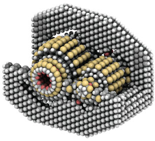 This is the SRG-I(c), a nanoscale speed reducer gear modeled using NanoEngineer-1. This gear assembly includes a pinion gear (small), an output gear (large), and a casing with embedded bushings that hold the two gears in place so that they mesh. The goal of the SRG-I(c) was to create a simple speed reducer gear with as few atoms as possible. Image courtesy of Mark Sims, Nanorex, Inc. |
Current Nano Applications
Toth-Fejel believes we are in the “stone age” of nanotechnology. “In nanotech, applications that have relatively disorganized size and surface effects are already on the market—I’m talking about nanoparticles, nanocoatings, and carbon nanotubes. The companies involved at this stage are working on increasing production while lowering costs.”
With nanoparticles and nano coatings there is slightly more engineering required to increase precision, since now we only have fairly high control in just one dimension. Carbon nanotubes (CNTs), allotropes of carbon with a cylindrical nanostructure, are a good example. They have been constructed with length-to-diameter ratios of up to 28,000,000:1, which is significantly larger than any other material. These CNTs are strong, with unique electrical properties, and are efficient conductors of heat.
The National Institute of Standards and Technology (NIST) did a study of the 50-100 carbon nanotube companies in the U.S. only to learn that there are many problems in the making and selling of carbon nanotubes. Zyvex Materials has developed a technique for embedding carbon nanotubes in epoxies, which would offer 10 percent greater material strength with only two percent loading.
Meanwhile, engineered nanoparticles like dendrimers, silsesquioxanes, and celluistic nanocrystals are poised to enter the market. A successful example of the use of nanocrystals is the nano pants, which offer stain resistance in dress pants and ties. This type of application is what’s known as “nano-enabled,” where some difficult engineering at the chemistry level is done so that the exact properties of a molecule being built is tightly controlled, adding 0.001 percent by weight of a material to a product, thereby significantly increasing the value of the final product.
Productive Nanosystems
Toth-Fejel’s area of interest is in Productive Nanosystems, currently making progress in the laboratory phase, with product demonstrations possibly five years out. The bottom-up approaches, like DNA Origami, need to build logic circuits complex enough to do error correction (like modern computers do), while top-down techniques like Patterned Atomic Layer Epitaxy need to bootstrap by using one probe to build another.
One of his current projects involves Pattern Atomic Layer Epitaxy, in which a scanning probe selectively removes hydrogen atoms from a silicon surface, and then allows another layer of silicon to deposit on the dangling bonds left behind. This top-down process is funded by DARPA for Zyvex, and expects to match the first phase of its research process in the next month or so.
Reducing Environmental Impact
Many people are concerned about nanotoxicity, which Toth-Fejel says is a valid concern, as additional surface area will make nanoparticles more reactive. This occurs because the surface area to volume ratio of particles grows exponentially as they are made smaller and smaller, meaning that more atoms (per pound) are exposed to the environment, especially the atmosphere or water. The result is that chemical reactions (such as oxidation) occur much faster. But on the other hand, researchers hold that nanotech will help reduce pollution and energy waste significantly in manufacturing, as it is more precise.
Nanoparticles tend to clump, which makes them difficult to produce. “When we engineer particles we’ll be able to make them so they’re biodegradable and make them more stable when we want them to be stable,” said Toth-Fejel. “Or vice versa. You can design at a level that will give more control over green processes, where you want less waste.”
Although respirocytes may make it possible for people to live longer, Toth-Fejel says that nanosystems might make it possible for people to get off the planet using the technology to develop low-cost launching platforms and systems.
Manufacture of solar energy cells has traditionally required a multimillion dollar facility to produce photovoltaic solar cells at 40 percent efficiency, prohibitively expensive for most people. Nanosolar is using nanoparticles to increase the efficiency of organic photovoltaic solar cells from 2 percent to 5 percent, thereby lowering the cost of solar electricity.
The researchers at NanoSolar are printing nano solar cells by the roll much like the garbage bags from grocery stores. To be able to build them with 40 percent efficiency roll to roll, could literally “change the world.”
Many different nanotechnologies are converging on the same basic concept—to control not just trillions, but kilogram quantities of atoms—and make them atomically precise.
More Info:
Molecular Manufacturing Enterprises
National Nanotechnology Initiative
NSTC (National Science and Technology Council)
Contributing Editor Susan Smith is DE’s expert in rapid technologies and has been immersed in the tech industry for more than 17 years. Send e-mail about this article to [email protected].
Subscribe to our FREE magazine, FREE email newsletters or both!
Latest News
About the Author
DE’s editors contribute news and new product announcements to Digital Engineering.
Press releases may be sent to them via [email protected].


