Pushing the Printed Electronics Envelope
The prospects are real, but we may have to wait a bit before we can experience the full benefit of additive manufacturing in electronics.
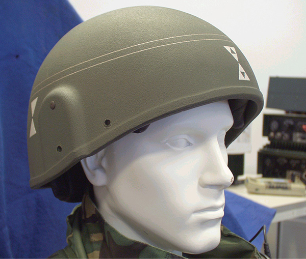
nScrypt’s SmartPump and the 3Dn printer promise to deliver the precision to enable design engineers to print complex, conformal circuits on most surfaces. The photo shows antennas printed along the top and sides of a rough-surfaced Kevlar helmet. Image courtesy of nScrypt.


Latest News
April 1, 2019
Printed electronics developers have started launching the technology into the third dimension, throwing off the constraints of flat, 2D architectures to integrate electronics directly into a product’s geometry.
Until recently, electronics companies designed and manufactured components, systems and layers in 2D. Then they finished off the lengthy process by performing steps like drilling, pressing and plating to connect the separate dies to create a multi-layer circuit board.
When you say, “3D circuit,” people still think of stacked planar circuits, perhaps connected vertically using vias. The inability to shake off the 2D mindset has slowed the evolution of printed electronics technology, limiting how engineers and software providers use the third dimension.
“Even though we have excellent 3D printers today, too many organizations are printing planar and conventional things,” says Raymond C. Rumpf, director of the electromagnetics and photonics lab at the University of Texas at El Paso (UTEP). “We are not doing as good as we could at innovating new things that 3D printing enables.”
This is not to say that developers of the technology lack a vision of what 3D-printed electronics can be; far from it. Current printing technology and recent research developments offer a glimpse of what 3D electronics might look like.
Two 3D Printed Electronics Visions
A look at some of the advanced printing technologies reveals differing perspectives on the form factors and architectures of 3D-printed electronics.
One of the most established methods of producing electronics is ink jet technology. These printers use an array of nozzles to propel small quantities of ink, typically using piezoelectric material to push the material through the small orifices. It delivers high resolution—enabling the production of crisp miniaturized components and traces—and good throughput.
One of the prominent providers of ink jet printers for electronics applications is Nano Dimension. “Nano Dimension’s systems leverage a layer-by-layer build approach,” says Simon Fried, co-founder and president of Nano Dimension USA. “It prints both the conductive material and the dielectric material, and so allows for a part to be built up with the two materials placed in X, Y and Z in accordance with the designer’s goals, starting from the bottom and building up in layers.”
Nano Dimension’s systems use two families of inks. Optimized for a range of applications—from radio frequency identification components to antennas—the AgCite family of nanoparticle inks promises good conductivity, adhesion and flexibility. Unlike regular metal powders that require high sintering temperatures, these inks can achieve a sintering temperature low enough to support a range of substrates, such as paper, polymer, glass and indium tin oxide.
The second family of inks uses a dielectric nanoparticle-polymer combination that provides electrical insulation down to hundred-micron widths. The inks are ultraviolet-cured as part of the print process.
An alternative approach uses a technology called microdispensing. These systems typically use positive pressure to transfer small amounts (microliters) of print material through a small tip or nozzle directly onto the desired surface. The technology often lacks resolution and accuracy. On the plus side, however, dispensing can deposit much thicker layers of materials with much higher particle loading. This can make building 3D parts faster. Additionally, metal provides structural support, and has higher conductivity.
A proponent of microdispensing, nScrypt, counters the technology’s shortcomings with the SmartPump, which controls the material volume flow at a pico-liter level (see video). This feature promises to enable precision printing at high print speeds, with clean starts and stops of the dispensing/printing path.
One of the advantages offered by SmartPump technology is the expanded, compatible range of materials. “nScrypt has an optimized nozzle that reduces back pressure and allows dispensing of an extremely wide range of material viscosity—from 1 cP to 1 million cP,” says Casey Perkowski, a mechanical engineer at nScrypt. “Meaning we can print materials as thin as water and thicker than peanut butter. This includes partial loaded materials with micro and/or nano particles. This gives us over 10,000 commercially available materials we can print.”
Another strength of the technology lies in nScrypt’s Factory in a Tool suite, which is bundled with the company’s 3D printing and microdispensing systems. The tools support multiple methods of depositing materials, offer features like pick-and-place (see video), and perform post-processing functions such as milling, polishing and laser processing. Factory in a Tool accommodates many types of materials, including materials with high particle loading.
Though nScrypt’s microdispensing technology is a layer-by-layer process, the Factory in a Tool suite allows the printing system to enhance 3D electronics production by interleaving disparate functions and processes throughout the operation.
“Building a 3D part works by alternating between the various tools during the print,” says Rumpf. “It may start by printing a few layers of fused filament fabrication (FFF) to form a dielectric substrate, then start printing layers with small gaps, switch to dispensing to fill the gaps with conductive ink, switch back to FFF to build another layer and so on until you have a 3D multi-material part. The machine may do some drilling or milling at various intermediate stages and place some electric components.”
Hurdles and Shortcomings
Though current 3D printing hardware is fully capable of producing 3D circuits, the transition to true printed 3D non-planar electronics has been slowed by the absence of adequate development tools. The reality is that the majority of investments and research still must be done in areas such as design practices, standards and manufacturing processes.
“Existing modeling and simulation software does not address 3D printed electronics directly, which can make design tedious and harnessing the extra capabilities of printing technologies difficult,” says Ken Church, CEO of nScrypt. “Many experts in 3D printed electronics design have found ways to use combinations of design software packages to achieve complex multi-layer devices, using features such as adjustable material properties through selective infill percentage in different areas, non-vertical vias and channels, embedded ICs [integrated circuits] and other design freedoms granted by the printing process.”
This approach handicaps development efforts, requiring designers to spend extra time making the workaround successful.
“Current tools can be used for designing these components, but it often takes extra effort on the part of the designer to understand how to apply certain features of the tools and use different CAD programs for different parts of the design,” says Vikram Lyer, a Ph.D. student in the electrical and computer engineering program at the University of Washington. “For example, electromagnetics simulators can model complex geometries, but the designer has to create those using the interface available within the program and then likely export it to a 3D modeling program for conversion to a different file format for fabrication.”
The absence of automation also limits the usefulness of this approach. “The current software allows for some conformal design—such as contouring traces to a surface—but the layout is tedious, and all connections are routed by hand,” says Perkowski. “The placement of components is difficult, and auto-routing of traces does not exist. Just as planar software for 3D printed electronics comes up short, 3D software is an even larger leap from traditional design software.”
What the industry needs is a new breed of design software tailored for the third dimension. “There is a need for a software that is a hybrid of 3D mechanical modeling software and electronics layout software,” says Church. “This would take in schematics of the electronic circuit, allow you to draw a 3D part and then place components in any orientation or position throughout the part, and route the conductive traces through the object.”
Filling the 3D Printed Electronics Software Gap
Defining the necessary software and providing the actual tools are two different things. Research groups and AM technology providers, however, have begun to develop and introduce software that attempts to bridge the gap between traditional design tools and 3D printed electronics.
For example, Nano Dimension offers two software packages targeting the 3D market. The first, a free add-in for SolidWorks, promises to provide a design environment optimized for 3D printing multi-material electronics (see video). The software aims to help engineers design complex prototypes—consisting of polymers and metals—that can be 3D printed on the company’s DragonFly Pro printer. The second, called Switch, offers a proprietary pre-processing application that enables operators to prepare printed circuit board designs for 3D printing on Nano Dimension’s printer.
On another front, researchers at UTEP have begun to develop software that goes beyond enabling the design of circuits that conform to a surface and opens the door for designing and manufacturing 3D/volumetric circuits.
The first software the UTEP research team developed is a CAD tool that lets engineers lay out 3D circuits and route interconnects. The tool helps place components in any position or orientation throughout all three dimensions. Interconnects of various types—such as high-frequency, power or thermal—can be routed to follow smooth splines.
The second program is a tool that generates hybrid G code from CAD files, with arbitrary multi-material structures. “This tool allows us to drive multiple tools from a single g-code file without having to manually code anything,” says Rumpf.
All of this came together during the summer of 2018, when the electromagnetic lab produced its first 3D/volumetric circuits. Of note is that these academic lab–based software systems are works in progress that have not been commercialized. Ultimately, the UTEP researchers plan to integrate all of the software tools and algorithms they have developed into a single, easy-to-use tool.
Rethinking Design of Electronics
Engineers pushing the limits of design to achieve the full potential of 3D-printed circuitry will have to approach the development process from new angles, and use new design rules.
“By rethinking traditional circuit design, engineers will have much more freedom in the shape of their designs, which will impact the size and look of the final product,” says Fried. “Additive manufacturing offers the opportunity to change the way electrical functionality is achieved, such as through printing passive components, as well as allowing for digital, radio frequency and passives to coexist within designs in ways that traditional manufacturing cannot attain.”
This means that designers will have to find new solutions for old issues. For example, heat management is already a problem in high-density and high-power electronics. Having embedded circuits precludes the use of traditional methods of managing heat like fans and heat sinks. For future printed structures, new heat management methods must be developed—possibly using micro-fluidic channels spread throughout the part to dissipate heat.
Engineers will also need to identify new ways of managing electromagnetic interference (EMI). “For EMI, ground planes and via fences are traditionally used to manage EMI in circuits,” says Church. “These are planar solutions and will need to be reimagined. For complex RF circuits, these are very important and have a large effect on performance. New concepts of how to do this—such as printing shielding around certain components and conductive traces—present challenges.”
The transition to 3D printed electronics also redefines the role of enclosures. “If you go back a few years, the only job of the enclosure was to hold the I/O and perhaps act as an EMI shield,” says Mike Dean, marketing director for Optomec, a manufacturer of Aerosol Jet Systems for printed electronics. “Today, designers are beginning to see the enclosure as an opportunity to extend the real estate of the printed circuit board. Components like antennas, sensors and interconnects can now live on the enclosure, which makes the overall device smaller and in some cases adds functionality.”
It’s clear 3D printed electronics promise to redefine each stage of the development cycle. The additive approach has the potential to change workflows, turbo-charge development cycles and introduce new ways to make the unmakeable.
More Optomec Coverage
Subscribe to our FREE magazine, FREE email newsletters or both!
Latest News


