
New printable inks allow sensor providers to manufacture ultra-thin devices in a range of sizes, shapes, and lengths. Shown here is Interlink Electronics’ FSR 402 Short Force Sensing Resistor, which has a 12.7 mm diameter active area and is available in four connection options. Image courtesy of Interlink Electronics.


Latest News
December 1, 2016
Sensors have begun to cast off their traditional forms, enabled by the emergence of a new class of materials and manufacturing techniques. This transformation has allowed developers to introduce sensors that change the way users interact with both the digital and physical worlds. Equally important, these new technologies have swept aside physical design constraints and in the process expanded the options available to engineers in the design of new products.
These developments stem from the desire of developers to meet market demands growing out of the emergence of the Internet of Things (IoT) and technologies like wearable devices. In an era in which electronics companies constantly push the envelope in terms of form factor, energy efficiency and economy, engineers must seek out new materials and manufacturing processes with which to build their sensors. Two materials that promise to play a major role in shaping the next generation of sensors are stretchable inks and graphene. While application of these materials currently seems to be focused on health care and wearable applications, the incredible properties of the materials almost guarantee that their influence will spread to other industries and applications.
A “Wonder Material” for Sensors
One of the most impressive of these materials almost defies description. It’s stronger than a diamond, but only one atom thick. Graphene promises to revolutionize future electronics, capitalizing on its extraordinary electrical conductivity, optical properties and thermal conductivity. These qualities also make the “wonder material” a natural candidate for sensor fabrication.
 Graphene is just one of several new materials used in the fabrication of electronic components that promises to change the form and function of sensors. The wafer shown here contains graphene field effect transistors, which enable chemical and biological sensors to detect selective species. Image courtesy of Graphene Frontiers.
While it has many applications, graphene has proven to be particularly effective in chemical and biochemical detection applications. Its large surface area enhances the surface loading of biomolecules, and its conductivity and small band gap are well suited for conducting electrons between biomolecules and the electrode surface.
Graphene-based biosensors can be used for a variety of tasks, including the detection of glucose, cholesterol and hemoglobin. The carbon material also holds great promise for electrochemical biosensor development, based on direct electron transfer between the enzyme and the electrode surface.
While it is relatively easy to create a chemical sensor or a biosensor, it’s another matter to build a sensor selective to different species. Graphene-based sensor designs have overcome this shortcoming by incorporating field effect transistors (FETs).
One vendor using this approach is Graphene Frontiers. Each of its chemical sensors and biosensors incorporates a FET, with a graphene channel. Receptor molecules or antibodies, depending on the type of sensor, are attached directly to the graphene channel.When binding events occur, the current through the transistor changes, and the signal can be analyzed to determine the concentration in the sample. Graphene Frontiers’ chemical sensors are only 10 mm wide, and as many as 25 analytes can be detected by a chip smaller than the size of a dime.
“Graphene’s stability, conductivity and two-dimensional nature make it ideal for sensor applications,” says Bruce Willner, chief executive officer of Graphene Frontiers. “These properties are essential for sensitivity and specificity … Our sensors are composed of graphene field effect transistors (GFETs), functionalized to detect specific chemicals and biochemicals. The target chemical is defined by the receptor attached to the GFET.”
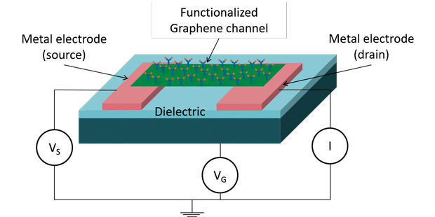 Graphene-based chemical and biological sensors incorporate field effect transistors to enable the sensor to identify specific species and quantify the concentration in the sample. Image courtesy of Graphene Frontiers.
Until recently, the main hurdle facing makers of graphene-based sensors was how to produce high-quality material, on a large scale, at low cost, and in a reproducible manner. The situation was compounded by the need for a complex chemical vapor deposition process. Large-scale production of graphene using crystalline epitaxy was problematic, and this was possible only on a metallic substrate, which restricted the use of graphene for electronics. Technological advances, however, have mitigated these obstacles.
Currently, the main factor hampering development of graphene sensors is the absence of standards. “Graphene, a new material, is difficult to specify,” says Willner. “There are no industry standards to define a graphene product or specify performance parameters. Accordingly, it is difficult to source consistent material. As a result, we [Graphene Frontiers] produce our own graphene for sensors in house. The graphene is the critical component in the sensor, and controlling this material is essential to reliable production.”
Graphene offers design engineers real options, opening the door for smaller and lighter sensors that can detect minute changes more quickly than traditional sensors. Graphene devices will also be less expensive. That said, the process of getting the most out of graphene in sensor designs, as well as production techniques, are just getting started.
What’s Next
While graphene holds great potential for the advancement of sensors, other materials are in the wings that will also shape sensor technology.
“Graphene is only the first of a growing family of two-dimensional materials,” says Willner. “While graphene development is more advanced and more stable than many of these other materials — such as hexagonal boron nitride and molybdenum disulfide — these other materials will have roles in designing custom structures for sensing.”
Printable and Flexible Sensors
The second materials to play a major role in shaping the next generation of sensors are stretchable inks, which enable the production of printed sensors, a new class of sensors that offer both form factor and cost advantages. Printed sensors offer features that are at the top of most engineers’ wish lists, including such things as small size, the ability to conform to a variety of surfaces, lower manufacturing costs, low power consumption and ease of integration with other functions.
 One of the major hurdles graphene-based sensor providers had to overcome was the development of processes that could economically mass-produce graphene. Graphene Frontiers’ proprietary manufacturing process creates a continuous graphene production and transfer line that enables the cost-effective manufacture of high-quality graphene films. Image courtesy of Graphene Frontiers.
A good example of one of these sensors is Interlink Electronics’ Force Sensing Resistor. This thin form factor device (0.45 mm) provides an inverse change in resistance in response to an increase or decrease in applied force, targeting human-machine interface applications. The Force Sensing Resistor consists of a polymer substrate, with the first functional layer taking the form of a conductive-carbon-based patterned circuit that serves as the sensor. On the underside of the next functional layer, you find a printed electronics network, which also serves as the encapsulant of the stack. These sensors are available in a range of sizes, shapes and lengths.
It is important to remember that these features are made possible, in large part, by improvements made to the composition of the inks used in the printing process. The blend of inks has three components. Printable semiconductor inks enable high-precision physical and environmental sensing, as well as analog signal and logic processing of sensing data. Electrochemical inks enable integrated energy storage for autonomous or semi-autonomous sensing networks. And thermoformable inks and substrates provide for the integration of sensing devices into different physical shapes and geometries.
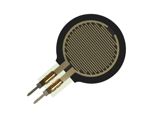 New printable inks allow sensor providers to manufacture ultra-thin devices in a range of sizes, shapes, and lengths. Shown here is Interlink Electronics’ FSR 402 Short Force Sensing Resistor, which has a 12.7 mm diameter active area and is available in four connection options. Image courtesy of Interlink Electronics.
Printing sensors is not new to the electronics industry, but advances in the technology now enable more types of sensors to be fully printed. This new breed of sensor can measure a broad gamut of parameters. These include chemical/gas composition, touch/force/pressure, temperature, humidity, bio-medical data, airflow and imaging.
Current printing processes—such as screen printing, flexography, gravure and inkjet—enable low-temperature processing and cost-effective manufacturing, especially on polymer-based flexible substrates. Digital manufacturing, which includes 3D printing and ink jet deposition, streamlines the production of the sensors by enabling direct translation of digital design data into fabricated prototypes and finished parts.
By combining the material and production technologies, sensor makers can fabricate flexible autonomous or semi-autonomous devices, which are well suited for many of the applications created by the emergence of the IoT.
“Implementation of these materials in sensing devices, in combination with new manufacturing processes, will allow design and manufacturing of intelligent and interactive surfaces,” says Albert Lu, chief technology officer at Interlink Electronics. “This will have a strong impact by enabling intuitive human-machine interface and machine-to-machine interface solutions. Design engineers should consider the novel approach of seamlessly integrating sensing devices as part of the industrial design flow and human factor engineering.”
Despite all of the coverage of printed electronics in the press, the technology is just emerging from the early stages of its development, and there are still some issues that have to be resolved. Big picture: The challenge for developers is that the printed sensors still need designs that provide for them. This will require additional design tools.
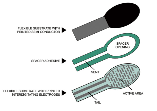 The process used to print sensors allows manufacturers to create devices by depositing multiple layers, combining substrates and layers of functionality. The end result is a small, flexible, feature-rich device with an array of functions. Image courtesy of Interlink Electronics.
“To improve the design cycle workflow, new multiphysics design automation tools would be very useful,” says Lu. “An example would be the tight integration of electronics circuit design and mechanical design.”
Changing of the Guard?
For so long, silicon has defined the form and function of electronics, and in doing so, the essence of sensors. That seems to be changing.
Materials like graphene, hexagonal boron nitride, molybdenum disulfide and new printing inks will open doors for the introduction of ever-smaller devices that out-perform their predecessors in terms of speed, sensitivity, and cost. What this means for the design of sensors is open to speculation. One thing is certain: Performance will continue to improve by leaps and bounds.
More Info
Subscribe to our FREE magazine, FREE email newsletters or both!
Latest News


