
Latest News
December 1, 2011
By Pamela J. Waterman
Getting a handle on nanotechnology is tricky, to say the least—both literally and figuratively. On a factor-of-10 scale, nanoparticles such as a DNA strand are about 10,000 times smaller than a red blood cell and 100,000 times smaller than a human hair. Or, as clarified so eloquently by Dr. Andrew Maynard in his Twinkie Guide to Nanotechnology video, comparing a DNA molecule to a Twinkie snack cake would give you roughly the same perspective as viewing a Twinkie sitting on Earth’s moon.
Though science and industry have worked with nano-sized particles for several centuries (think colloidal gold giving color to stained glass windows in French cathedrals), this field of study couldn’t really take off until the advent of scanning electron microscopes. But “seeing” nanoparticles is one thing—manipulating them, understanding them and using them in new ways is another. As with so many other fields of science and engineering, predicting material behavior with computer simulations can be not only insightful, but an absolute necessity. DE looks at the basics of nanotechnology, why it’s increasingly important, and some current work done with nanotech simulations.
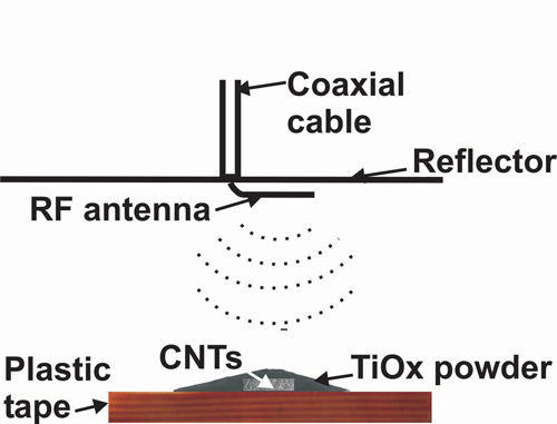
Schematic of direct growth of CNTs on plastic tape via selective heating. RF
power is predominantly absorbed inside TiOx powder. Hydrocarbon gas is
heated while diffusing between loosely packed TiOx particles and decomposes
on the tape surface patterned by catalytic nanoparticles. The resulting carbon
atoms assemble vertically oriented CNTs via endothermic catalytic reactions.
After the CNT growth, the TiOx powder is washed off.
Image courtesy CFD Research Corp.
A Nanotech Primer
Nanotechnology, or nanotech, or the-science-of-the-extremely-tiny, involves the study of materials and physical interactions of particle sizes ranging from 1 nm to 100 nm. From a practical point of view, nanotech is the combination of chemistry and mechanical engineering that can manipulate and control materials and interactions at the level of atoms and molecules.
A very readable overview of this subject is presented by the Project on Emerging Nanotechnologies (PEN), a program established in 2005 as a partnership between the Woodrow Wilson International Center for Scholars and the Pew Charitable Trusts, of which Dr. Maynard was chief science adviser. He now leads the University of Michigan Risk Science Center. PEN collaborates with researchers, government, industry, non-governmental organizations, policymakers and others to look at all aspects of nanotechnology long-term, identify gaps in knowledge and regulatory processes, and develop strategies for closing them.
Why is this important? Nanoparticles, already in use in more than 1,300 consumer products, hold tremendous promise for improved processes and products that may involve close, everyday encounters. Their very small size may allow them to get into places that larger particles can’t go. This could be good for, say, creating medicine that travels deeply into a brain tumor, but could be bad if they pose inhalation or environmental risks. Science and industry need to “get it right” to make sure producing and using these materials is beneficial, not problematic—and much work is already under way.
Why Nanotechnology
At the nanoscale, researchers can directly control material properties, making them lighter, harder, more rugged or improved in seemingly uncountable other ways. Just making things on a nanoscale may cause a chemical to change color or start conducting electricity. Nanoscale particles (which come in dozens of shapes) tend to be more chemically reactive than the same materials at the bulk scale, because they generally have more surface area and a greater portion of their atoms in close proximity to their surface. Even within a single chemical compound, researchers have seen nanoparticles shaped as rings, tubes, hexagons, brushes, ovals, helices and ribbons. Each of these has the potential for different applications, because shape determines behavior.
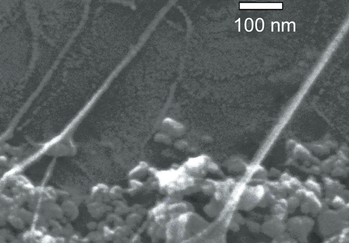
A typical scanning electron transmission microscope image of deposited CNTs
on the overall intact kapton tape. Some bubbling on the surface of the tape was
detected, indicating that the surface temperature was near the melting point
of kapton.
Image courtesy CFD Research Corp.
Sample nanoparticle and nanofiber applications already in use include clear zinc-oxide sunscreen, anti-microbial socks, water- and stain-resistant trousers, nano-structured organic light-emitting-diode displays, plastic containers that extend the lifetime of food, lighter/stronger tennis rackets and carbon-fiber conductive gloves for operating touchscreens in cold weather. By 2014, the global worth of nanotech products is projected to be $2.25 trillion.
Research is well under way applying nanotechnology to targeted drugs for treating cancers, Parkinson’s disease and cardiovascular disease, showing promise for success without side effects. Carbon nanotubes are so strong that scientists are working with them to create T-shirt-weight bulletproof vests. Nano-oxide particles have been tested for in situ oil-spill remediation projects. Solar panels built from nanotech devices may be far more efficient and lighter than current versions, and fiber-optic bundles seem to transmit with lower losses when nanometer-slots are built into fiber cores.
Simulation Programs
Simulating the behavior of nanoparticles (creating them, moving them, influencing them) or of nanomaterials (fluids, composites, etc.) is a challenge for traditional finite element analysis (FEA) and computational fluid dynamics (CFD) software. How do they flow, connect, absorb gases, respond to temperature, and conduct electricity? Do these parameters change for every different nanoshape? In many cases, the laws of quantum physics take over from Newtonian physics, so defining even basic material properties becomes a challenge—and solver math may have to change.
Barry Zorman, a Phoenix-based consultant who has worked in nanosimulation, notes, “From a mechanical design point of view, it is still very challenging for computer simulations to include nanoscale or molecular scale detail, along with the much larger structural features that also determine a real complex material’s mechanical properties.”
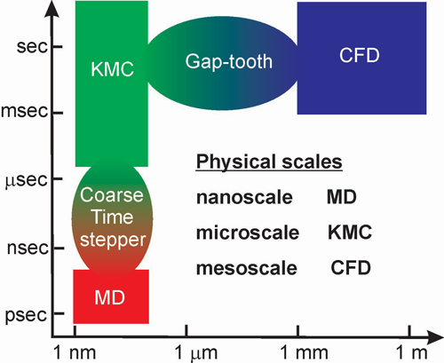
Performing simulations with nanomaterials requires accounting for their behavior
across different scales. CFD Research Corporation has developed a Multi-Scale
Computational Environment that integrates tools for molecular dynamics (MD),
Kinetic Monte Carlo (KMC) analysis and Computational Fluid Dynamics (CFD),
including proprietary “bridging” software. Image courtesy CFD Research Corp.
Resources in the Nanotech Associations/ Directories/Initiatives/Test Facilities
LinkedIn Groups
Market/Product Reports InnoResearch.net: “Production and Applications of Carbon Nanotubes, Carbon Nanofibers, Fullerenes, Graphene and Nanodiamonds: A Global Technology Survey and Market Analysis,” Innovative Research and Products Inc., Report Code: ET-113, February 2011. An exhaustive look at the field of nanocarbon materials, including profiles of more than 180 companies manufacturing nanocarbon materials and companies that manufacture products using these materials. NanoTechProject.org/iphone: iNano, the new iPhone application from the Project on Emerging Nanotechnologies. It lists everyday nano-items in the Nanotechnology Consumer Products Inventory. Nanotech-related Conferences Nanoinformatics 2011, Dec. 7-9, 2011, Arlington, VA |
Because of the potential benefits and fundamental fascination of nantotechnology, dozens of organizations have addressed these issues, and many offer simulation assistance. nanoHUB.org, for example, is a group that encompasses opportunities within the nano community to share, publish, teach, research, collaborate and learn across the spectrum of technologies. Its website states, “We believe that modeling and simulation is, in general, underutilized in both research and teaching.” To improve that situation, the site provides more than 160 online simulation tools that run like applets. They include a nano Materials Simulation Toolkit, the MIT Atomic Scale Modeling Toolkit, and a Carbon Nanotube MEMS Relay Simulator.
Nanotechnology research centers are located at government research laboratories and major universities worldwide. In the United States, the former includes five Nanoscale Science Research Centers founded by the U.S. Department of Energy (such as the Center for Functional Nanomaterials at Brookhaven National Lab). The latter includes university members of the National Science Foundation (NSF)-founded National Nanotechnology Infrastructure Network.
Several other academic centers (with some areas of specialization) include:
- University of Wisconsin-Madison Center for NanoTechnology (nanobiology, nanolithography);
- University of Massachusetts-Amherst Center for Hierarchical Manufacturing (university-to-industry transfers; roll-to-roll printed electronics processing);
- Virginia Polytechnic Institute and State University (a member of the NSF-funded Center for the Environmental Implications of Nanotechnology ]CEINT] at Duke University); and
- University of Akron Goodyear Polymer Center (adhesives; nanofiber wound-healing bandages; ceramic nanofiber filtration).
Simulation Options
Many groups address the multi-scale challenges of nanosimulation mentioned by Zorman; details of one such methodology and its proponents are at Quasicontinuum.
However, the commercial world has also been busy in this field for years, though possibly under the general radar. CFD Research Corp., or CFDRC, provides advanced simulation software and consulting services for the analysis, design and optimization of nanomaterial fabrication processes. Customers may seek the company’s help, for example, in determining the best initial conditions for growing carbon nanotubes on a substrate.
“The problem with (manufacturing) nanomaterials is that their outstanding features are formed at nanoscales, and you have to account for all these different scales during the growth,” notes CFDRC Principal Scientist Alex Vasenkov. To manage this issue, the company has developed a multi-scale computational environment integrating standard CFD tools with Kinetic Monte Carlo (KMC) and Molecular Dynamics (MD) software.
The key to this successful approach is CFDRC’s creation of two bridging modules, or “gap tools,” that transfer the results between each pair of analysis tools. Analyses for materials beyond carbon (such as metal alloys and ceramics) are in the works. It’s a complicated process. Trust me—you’ll want to talk to these people.
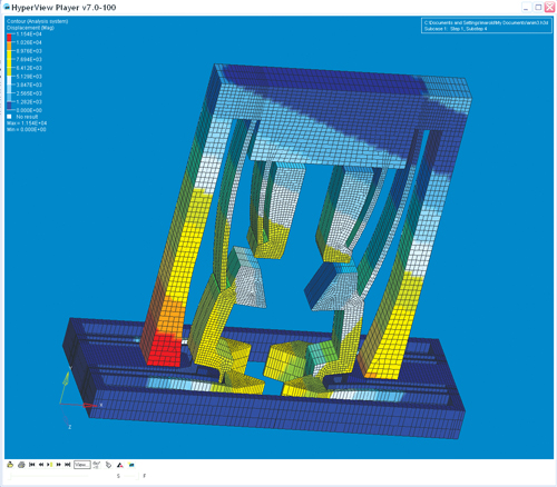
Meshed model of nanoscale microconductor ready for finite element analysis,
created with Altair HyperMesh software; FEA results presented in Altair HyperView.
Image courtesy Altair Engineering and Zyvex Instruments.
COMSOL Multiphysics simulation software has also been a key tool for numerous users working in nanotechnology applications, as seen by the titles of papers presented in recent years at the COMSOL annual conference. Study topics have included biomedical applications of micro- and nano-electromechanics, multiphysics simulation of cancer therapy using carbon nanotubes (CNTs) and near-IR irradiation, the behavior of ionic currents through an electrolyte-filled CNT, and microfluidic/heat transfer/chemical behaviors in nanophotonic devices.
Altair’s HyperWorks family of CAE software plays a big role in product development at customer Zyvex Instruments, a division of DCG Systems. The company creates devices that physically grip and manipulate parts during micro-electro-mechanical systems (MEMS) assembly, which in turn can help with nanotech fabrication. Zyvex mechanical engineer Aaron Geisberger says he has found HyperWorks’ open architecture useful in his workflow, because he can customize HyperMesh templates for non-experts to help with intensive meshing tasks. Post-processor HyperView has also let his group visualize the finest details of FEA results.
Speaking of fine details, QuantumWise, a Danish company with U.S. representation, offers atomic-scale simulation software targeted to electrical properties. The company notes that many application areas in nanotechnology are related to effects occurring at junctions, interfaces and surfaces, and that it is critical to accurately model such phenomena from quantum theory. Its Atomistix ToolKit (ATK), in use since 2006, handles complex nanostructures—combining molecules with periodic systems and macroscopic elements. The software has been applied to work with such materials and devices as graphene, nanotubes, nanowires and single-electron transistors.
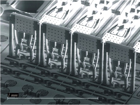
SEM image of nanoscale micromachined connectors assembled vertically
into micromachined silicon sockets, with close-up view. Zyvex Corporation
used Altair HyperMesh to develop FEA models and Altair HyperView for
results visualization. Images courtesy Altair Engineering and Zyvex Instruments.
Always Room for Improvement
A parting perspective on computer simulation in nanotechnology comes from Stan Prybyla, a Ph.D. in physical chemistry and president of Breakthrough Technology Development. His consulting firm specializes in using statistical design of experiments (DOE) to help businesses zero in on the best manufacturing parameters for producing nano-composite materials.
“There’s a wealth of opportunity for discovery and utilization in nanotech product development,” observes Prybyla. “Development of modeling techniques beyond the empirical techniques will help us get to the next stage of development of these materials.”
Contributing Editor Pamela Waterman, DE’s simulation expert, is an electrical engineer and freelance technical writer based in Arizona. You can send her e-mail to [email protected].
MORE INFO
NanotechProject.org/news/archive/the_twinkie_guide_to_nanotechnology
Subscribe to our FREE magazine, FREE email newsletters or both!
Latest News
About the Author
Pamela Waterman worked as Digital Engineering’s contributing editor for two decades. Contact her via .(JavaScript must be enabled to view this email address).
Follow DE

