Optomec Releases Software for Production 3D Printed Electronics
Software enables fully automated process sequencing for advanced 3D semiconductor packaging.
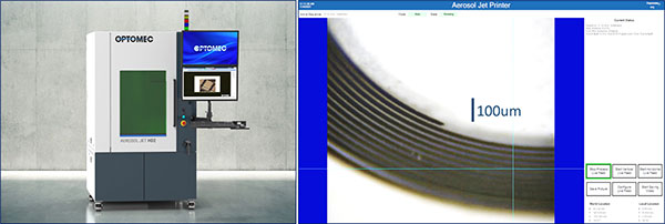
The new HD2 Aerosol Jet® Printer is optimized for high volume printed electronics production. Image courtesy of Business Wire.


Latest News
March 17, 2023
Optomec, manufacturer of 3D electronics printers, has released a new production control software product designed specifically for high-volume manufacturing of printed electronics.
The software, called KEWB, draws on the field experience of Optomec’s 400 installed Aerosol Jet industrial printers, and was designed for Optomec’s high-volume production customers with applications such as multi-chip packaging, mm-wave interconnects, heterogenous chip integration and 3D printed antennas for 5G devices.
KEWB incorporates enhanced operator guidance, powerful vision and alignment tools, extended runtime process control , and industry 4.0 connectivity to meet the demands of world-class manufacturers. Additionally, KEWB includes a powerful scripting capability that enables automated sequencing of all critical process steps for continuous inline production; ie: load, scan, align, print, inspect, unload, etc.
The release of the KEWB software follows the recent introduction of the Aerosol Jet HD2 printer, a printed electronics and material dispense platform that combines high-speed, sub-micron resolution, SEMI-compliant inline conveying and advanced alignment optics over a 300x300 mm work area.
“The new KEWB software simplifies everything—from process integration to operation sequencing to maintenance,” says Dave Gleason, software development manager at Optomec. “In addition, it’s configurable for multiple user levels, so the engineer sees a full vision tool kit while the machine operator sees a simplified, pictorial sequence of process steps. The entire software approach is focused on production.”
Optomec’s printed electronics machines enable manufacturers to create 3D electronic structures—such as circuits, sensors, antennas and interconnects—with features as small as 10 microns using nanoparticle inks.
Sources: Press materials received from the company and additional information gleaned from the company’s website.
More Optomec Coverage
Subscribe to our FREE magazine, FREE email newsletters or both!
Latest News
About the Author
DE’s editors contribute news and new product announcements to Digital Engineering.
Press releases may be sent to them via [email protected].