Helping design and engineering professionals discover, evaluate and specify technologies and processes that shorten the design cycle and enable success.

Digital Engineering April 2026
In the latest issue of Digital Engineering, we take a look at the latest innovations in design for additive manufacturing, including the use of natural language inputs, social media cosplayers, and AI integration. The issue also includes a feature…

January Special Focus Issue: Design for Additive
In this Special Focus Issue of Digital Engineering, learn about the latest advancements in design for additive manufacturing, including new software tools, additive in automotive, custom medical devices, and more.
Decades ago, the world of diagnostic single-exposure X-rays was supplemented with the layer-by-layer, 3D density details generated by microscale X-ray computed tomography (microCT) imaging. Just as engineers have long used standard X-rays to examine the internal structure of traditionally manufactured parts, developers and quality assurance groups have more recently applied the deeper capabilities of microCT to parts produced by additive manufacturing (AM).
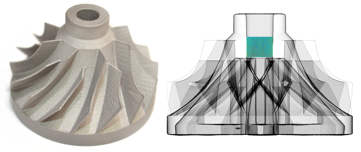
One of the many benefits of metal AM is the ability to produce internal structures. Parts must not only meet dimensional specs but also display consistent and acceptable quality characteristics, such as high density and the absence of internal defects. MicroCT is a powerful tool for these and other AM applications, too, as described in a recent paper by Anton du Plessis et al, “X-Ray Microcomputed Tomography in Additive Manufacturing: A Review of the Current Technology and Applications” (Anton du Plessis, Igor Yadroitsev, Ina Yadroitsava, and Stephan G. Le Roux, 3D Printing and Additive Manufacturing; July 30, 2018). The paper offers worthwhile reading and includes a table comparing the types of microCT scan approaches/capabilities and corresponding time investment needed for a given evaluation goal.
While prototype and sample parts can always be physically sliced (destroyed) and imaged to expose internal details (which may be fine for plastic AM parts), non-destructive inspection is highly desirable for qualifying and verifying aerospace, automotive and medical final products.
MicroCT systems employ either a fan-beam or cone-beam approach to transmit X-rays through a part. Typically, the part (rather than the source) is moved incrementally on a rotary table, capturing hundreds or thousands of radiographs over a 180° or 360° rotation. Data from either type of scanner is collected at a planar detector and then processed to create 3D volume reconstructions, which can be analyzed and viewed layer by layer. Different densities of material show up as different gray shades across the images, generally capturing details down to three microns, with some high-resolution microCT scanners comfortably imaging down to 0.5-micron voxel size. MicroCT equipment can inspect metals ranging from aluminum and titanium to heavier alloys such as stainless steel and Inconel, primarily depending on the energy of the X-rays emitted by the source.
The video above shows a MicroCT scan of metal additive manufacturing feedstock powder. Scan duration was 2 hours at 2 μm voxel size. Generally, tens of thousands of particles are imaged in a single scan, and statistics on foreign particle contamination as well as particle size, shape, and porosity can be determined. Video courtesy Expanse Microtechnologies.
The applicability of microCT spans a large part of the overall AM process including characterization of feedstock powders, optimization of build process parameters, and inspection of as-printed or post-processed parts. With powders, microCT image data can be used to detect foreign particle contaminants as well as measure particle size and shape distributions and detect porosity internal to particles.
The video above shows that metal feedstock powder for additive manufacturing can be scanned using microCT and characterized in terms of particle size, shape, and porosity. A single 100 μm diameter particle is extracted from a microCT scan of several thousand particles and rendered in this animation. Porosity within the particle is highlighted in blue. Video courtesy Expanse Microtechnologies.
Build process parameter optimization can be accomplished by a systematic study of the effect of different parameter settings on a desired metric (porosity, surface finish, etc.) measured on carefully designed test coupons tailored for microCT inspection. For as-printed or post-processed parts, a wide range of measurements can be made including those for surface and dimensional metrology or for the size, shape, and spatial distribution of internal voids.
The video above shows that Metal 3D printed tensile coupons can be scanned prior to mechanical testing to reveal information on sample density as well as size and position of pores within the gauge length. (Right) 3D minimum intensity image showing porosity within the gauge length. Samples shown have a 6 mm diameter printed in Inconel 625. Scan duration was 90 minutes per vertical segment, with three vertical segments required to capture the full gauge length. Image courtesy Expanse Microtechnologies.
The main drawbacks to wider use of microCT within AM include cost and lack of standards (per article by Du Plessis et al). However, with careful application it can be a powerful tool to accelerate process development, leading to shorter timelines and cost savings compared to conventional approaches. Work on creating standards has included guidelines on how to seed natural flaws into test parts and therefore demonstrate ability to detect these flaws. There is also much discussion of pros/cons of test coupons: standard parts such as 10mm cubes or 15mm-diameter cylinders may vary due to build orientation and build parameters, yet higher resolution imaging is possible on smaller test parts.
Looking for an in-depth understanding of CT technology and its use in AM? Consider signing up for a new training course recently announced jointly by The Barnes Group Advisors (TBGA) and Expanse Microtechnologies. TBGA applies its 120-years of combined expertise in AM, aerospace requirements, research and development, and highly complex product development toward helping companies devise AM adoption strategies. Expanse Microtechnologies offers high-resolution X-ray CT imaging and unique, customized analysis services specializing in AM and advanced materials. The company’s staff have more than 70 years’ combined experience in microCT and the development and processing of advanced materials.
This new training course is offered as either a webinar or in-person workshop. It covers a range of topics designed to assist in the integration of CT in AM as part of an overall goal to foster the integration of AM into a client’s facilities, products, and design thinking. The topics of this training course are described in greater detail below. The content is modular and can be tailored to the unique needs of the client company.
An introduction to X-ray computed tomography highlighting the fundamental physics of X-ray imaging is provided. An overview of the process from planning to reporting is detailed to familiarize learners with the necessary steps to acquire trustworthy images and measurements. With this knowledge, students will understand the working principles and common applications of CT.
The primary applications of CT are presented relevant to both part inspection and material and process development. The focus is on introducing learners to specific characteristics of the sample that limit CT applications and on providing basic knowledge on the spectrum of CT capabilities.
An introduction to the relationships between sample size, image resolution, sample material and relative cost for CT scanning is discussed. The most significant differences among CT machines are highlighted to help learners understand both the trade-offs among major characteristics of CT inspection and what can be practically achieved using CT inspection.
An overview of the most important factors to consider when purchasing CT equipment for a specific application is provided using a case study to provide real world context.
Design can greatly affect the ability to inspect parts and test artefacts non-destructively. The aspects of good and bad designs relative to compatibility with CT inspection are discussed.
Best practices for obtaining helpful information from a CT machine supplier are discussed as well as consideration to the challenges and maintenance requirements of owning CT equipment. Guidance on choosing a CT service provider is also discussed.
During the course, students have access to specialist members of both the TBGA's ADDvisor Services and Expanse Microtechnologies’ teams.

Pamela Waterman worked as Digital Engineering's contributing editor for two decades. Contact her via DE-Editors@ digitaleng.news.
Follow DEJoin over 90,000 engineering professionals who get fresh engineering news as soon as it is published.


About Us · Contact Us · Editorial Team · Advertising · Privacy Policy · Subscriber Services · © 2026 Digital Engineering 24/7 · Peerless Media