Helping design and engineering professionals discover, evaluate and specify technologies and processes that shorten the design cycle and enable success.

May 2026 Special Focus: Artificial Intelligence in Design and Simulation
In this Special Focus Issue, learn about the latest developments in the integration of artificial intelligence into engineering workflows.

Design & Simulation Software Guide 2025
In this Special Issue, Digital Engineering presents its second annual guide to design and simulation software vendors.
When Juniper Networks, a manufacturer and developer of internet networking productsbased in Sunnyvale, California, designed a new router, project leaders decidedto build a prototype to test its initial design, checking to see if it would complywith electromagnetic compatibility (EMC) specifications. The EMC prototype consistedof two boards connected with 1.5 in. mechanical standoffs and another PCB thatinterfaced to card edge connectors on the two main boards. Testing the prototypeshowed emissions in the 4GHz range that were barely within design specifications,and the engineering team was concerned that manufacturing variations might pusha percentage of production over the limits and force the design to be reworkedor scrapped altogether.
Clearly, the company had to improve EMC performance, but its engineers faceda time-consuming process as they experimented with the prototypes in an effortto solve the problem. Aside from the time dedicated to making changes to the model,they knew that in some cases, changes to the prototype would prove expensive.
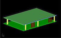 Left: Model of Juniper Networks product with outer enclosure show in hidden lineview.
Another limitation of this traditional method was that the team was only ableto measure emissions at the limited number of locations where they were able toplace a loop probe. Because of that, the test results didn't provide enough informationfor engineers to figure out how to make improvements.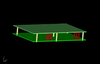
"We were right in the middle of this problem when we heard about FLO/EMC," saysJohn Lockwood, EMC engineer for Juniper Networks. A Flomerics sales call coincidedwith the project. "We spoke to the developer and they agreed to let us try outthe software at no cost on this problem. Because we had to meet a tight developmentschedule, we got started immediately."
Solving Problems Cheaply
FLO/EMC from Flomerics Inc. (Southborough, MA; flomerics.com) provides an analysis environment for simulating electromagnetic interactionsin and around electronic equipment to generate quick solutions for tough designproblems. It gave the project's engineers the ability to simulate the key componentsof their prototype—two high-speed logic boards and connectors—using new softwarespecifically designed to help designers address EMC compatibility problems.
By making that possible, FLO/EMC means engineers can identify EMC design issuesearly in the design cycle, well before complete physical prototypes are built.And the program differs from general-purpose electromagnetic simulation softwareby using the Transmission Line Matrix (TLM) method for solving Maxwell's equations.This provides major advantages when performing EMC simulations. First, the TLMmethod solves for all frequencies of interest in a single calculation and, therefore,captures the full broadband response of the system in one simulation cycle. Thisis particularly helpful with EMC analysis since potential resonances and emissionsvary over a wide frequency spectrum. Second, the TLM method creates a matrix ofequivalent transmission lines and solves for voltage and current on these linesdirectly. This uses less memory and CPU time than solving for E and H fields ona conventional computational grid.
Simulating the Design from an EMC Standpoint
Lockwood began by using the software to create an EMC model of the design. "Idiscovered early in the modeling process that you need to pay close attentionto the trade-off between detail and solution time," Lockwood says. "Simulatingevery detail of the design would have resulted in a model that takes days to solve,which is too slow to have a real impact on the design process." Instead, he says,they had to maintain the accuracy of the model by removing as much of the detailas possible while maintaining the features that had the biggest impact on EMC.
Below, right: Map of the surface currents in the smaller top board design withthe top of the enclosure cut away.
Using trial and error, Lockwood discovered that he could accurately simulatethe EMC performance of the product without modeling the individual componentson the PCBs or the dielectric layers. He also tried removing some of the mechanicalstandoffs between the two boards, but discovered they had to remain in order tomaintain accuracy.
"The result was a model that took about two hours to solve," he says, "and correlatedvery well to the prototype." Not only did the model accurately predict frequencyand the location of electromagnetic emissions, but it also duplicated the team'sexperience in terms of the model's sensitivity to design changes. "We knew fromtesting that if we insulated or disconnected some of the standoffs, the noiselevels were reduced—and the simulation predicted the same thing," says Lockwood.
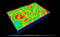
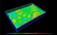
Freed from the need to build a new prototype to evaluate each design change,the team modified the model to evaluate how emissions were affected by changesto various design parameters. Lockwood says this allowed him to quickly modifythe model to evaluate a new design and adds that the simulation results providedfar more information than prototype testing. For example, it gave engineers acomplete map of the electromagnetic fields throughout the solution domain.
"We were a little perplexed at why disconnecting the grounds in the standoffsreduced the noise," Lockwood says. "We started doing things like increasing thenumber of grounds and making the ground returns wider to get a better understanding.We discovered that the source of the noise was actually ICs on the main boardpulling current from the power supplies on the top board and that the standoffswere adding extra ground returns in addition to the returns in the card edge connectors."The dimensions of the daughter card were such that at a high multiple of the mainclock on the primary board the whole structure tuned up. Insulating the standoffsforced the current to move in a tighter loop. Mechanical considerations made itimpossible to remove standoffs and insulating them with nylon would have presenteddurability concerns, but engineers made incremental improvements by changing sixstrips of ground in the connector card to one wide strip.
Finding a Zero-Cost Solutions
"The simulation also provided field maps of the inside of the cavity and we couldsee how inadvertently the original design had focused energy on the seams in theshielding," Lockwood says. "We would never have gotten this critical piece ofinformation, which proved the key to solving the problem, from physical testing."
By simulating the prototype, engineers got a color-coded 3D image of the cavity,which gave them a better understanding of the emissions than they would get usinga loop probe. They saw that the power planes on the upper card did not have togo to the end of the boards. "In traditional PCB manufacturing," he says, "theground and power planes go to within 50 thousandths of the edge, but that isn'ta requirement in most cases." On the next board revision, the engineers stoppedthe power at the edge connector, leaving off a half-inch long strip the lengthof the board. This moved the EMI source farther from the weak point in the shieldingand provided a big improvement since the design was already tightly coupled. Thenoise level immediately dropped from close to the limit to a "very healthy marginof safety" to a point where EMC is no longer a concern.
"We took this very visible demonstration of the effectiveness of EMC modelingto management and had no difficulty convincing them to purchase the software,"says Lockwood. "We have since used it on several other problems with very similarresults."
Jerry Fireman is the president of Structured Information, a marketing communications consultantfor the technology industries in Lexington, Mass. John Lockwood is the EMC engineer for Juniper Networks. You can contact the authors about thisarticle via e-mail; sent to [email protected].

DE's editors contribute news and new product announcements to Digital Engineering. Press releases may be sent to them via [email protected].
Follow DEJoin over 90,000 engineering professionals who get fresh engineering news as soon as it is published.


About Us · Contact Us · Editorial Team · Advertising · Privacy Policy · Subscriber Services · © 2026 Digital Engineering 24/7 · Peerless Media