Helping design and engineering professionals discover, evaluate and specify technologies and processes that shorten the design cycle and enable success.
Alert!
Digital Engineering ceased publication on July 1, 2026. This website remains available as an archive of engineering content.
For inquiries or information, please email [email protected].

May 2026 Special Focus: Artificial Intelligence in Design and Simulation
In this Special Focus Issue, learn about the latest developments in the integration of artificial intelligence into engineering workflows.

April 2026 Special Focus Issue: Generative Design
In this Special Focus Issue, Digital Engineering takes a look at how generative design solutions can be used across different types of design problems and with a variety of manufacturing approaches to accelerate design space exploration, and…
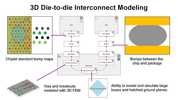
Keysight Technologies, Inc. launches 3D Interconnect Designer, a new addition to its Electronic Design Automation (EDA) portfolio. The solution addresses the complexity of designing 3D interconnects for high-chiplet and 3DIC (3D integrated circuit) advanced packages used in AI infrastructure and data center applications.
Keysight EDA software offers a workflow for designing and optimizing 3D interconnects accurately, according to Keysight. The tool handles complex geometries, including hatched or waffled ground planes. By enabling engineers to quickly design, optimize, and validate 3D interconnects used in chiplets and 3DICs, it minimizes iterations and speeds time-to-market, Keysight explains.
Key benefits include:
The solution integrates with Keysight's EDA tools as well as supporting the standalone version. When combined with Chiplet PHY Designer, engineers can design and optimize 3D interconnects specifically for chiplets and three-dimensional integrated circuits (3DICs).
“With today's complexity, manual 3D interconnect design and optimization have become a significant bottleneck," says Nilesh Kamdar, EDA Design and Verification general manager at Keysight. "By streamlining the process and providing early insights into potential issues like signal and power integrity, we're enabling engineers to get products to market faster and deliver compliant designs on tighter timelines.”
Resources
Sources: Press materials received from the company and additional information gleaned from the company’s website.

Keysight Technologies Inc. (NYSE: KEYS) is the world's leading electronic measurement company, transforming today's measurement experience through innovations in wireless, modular, and software solutions.
DE's editors contribute news and new product announcements to Digital Engineering. Press releases may be sent to them via [email protected].
Follow DE


About Us · Contact Us · Editorial Team · Advertising · Privacy Policy · Subscriber Services · © 2026 Digital Engineering 24/7 · Peerless Media