Helping design and engineering professionals discover, evaluate and specify technologies and processes that shorten the design cycle and enable success.


May 2026 Special Focus: Artificial Intelligence in Design and Simulation
In this Special Focus Issue, learn about the latest developments in the integration of artificial intelligence into engineering workflows.

April 2026 Special Focus Issue: Generative Design
In this Special Focus Issue, Digital Engineering takes a look at how generative design solutions can be used across different types of design problems and with a variety of manufacturing approaches to accelerate design space exploration, and…
One of the more compelling innovations in consumer electronics, and smartphones in particular, is the fingerprint scanner used for identity management. While most leading devices leverage capacitive technology, ultrasonic sensing, best known in the health care industry, is making an appearance in newer models thanks to its potential for advanced security.
The number of smartphones expected to ship with a fingerprint sensor by 2020 is estimated to be around 1.6 billion. However, before ultrasonic sensing can be established as a defacto cell phone feature, manufacturers face a long development road, in part because the technology is categorized as a MEMS, a miniaturized micro-electro-mechanical system. While traditional electronics devices could be designed and simulated with electronic design automation (EDA) tools, MEMS, due to their small size and sheer complexity, have never benefited from a codified simulation workflow, which complicates development and promotes a reliance on costly physical prototypes. Because the need for multiple, highly-coupled physics simulations push the boundaries of traditional design processes and CAE platforms, manufacturers interested in ultrasonic sensing are looking for a better way.
OnScale, a pioneer of on-demand, scalable simulation software, is doing its part to map out new simulation processes for MEMS, and for ultrasonic sensing, in particular. The company recently published a white paper titled, “Accelerating Ultrasonic Fingerprint Sensor R&D with Cloud Simulation,” to prove that cloud-enabled simulation can deliver the horsepower for telecommunications and security industry companies looking to whittle down the number of costly and time-consuming physical prototypes. Using cloud simulation to rapidly and virtually prototype MEMS devices like ultrasonic fingerprint sensors could help companies save millions of dollars in R&D costs in addition to shaving significant time off of development efforts.
“Solvers are limited by what they can do on a laptop or a desktop because you are physically constrained in the problem size you can tackle and how long it will take,” explains Dr. Gerry Harvey, vice president of engineering at OnScale and one of the co-authors of the white paper. “With access to supercomputers on demand, the problem you are testing can be oversized.”
So for example, if a simulation, such as one for ultrasonic sensing, required 1,000 core machines and 100 terabytes of RAM, the engineering organization wouldn’t need a comparable machine on site to get the job done—an imperative since most companies can’t afford or don’t have access to that kind of computing muscle. “With OnScale, you can create [a large-scale simulation] on demand in the cloud, get results, and shut it down,” Harvey says. “All you pay for is time used on the machine.”
In the ultrasonic sensor example, the OnScale platform enabled the research team to perform a full 3D simulation of a 110 x 56 PMUT array embedded fingerprint sensor designed and prototyped at the Berkeley Sensor & Actuator Center. The complete model consisted of 130M degrees of freedom and was solved on an AWS cloud with OnScale’s time-domain multiphysics capabilities (fully-coupled piezoelectric and elastic wave solvers) running 29 minutes per image, using 106 parallel cloud nodes. Each node tapped into 40 processor cores and 9.2 GB of RAM for a total resource allocation of 4,240 processor cores and 975 GB of RAM.
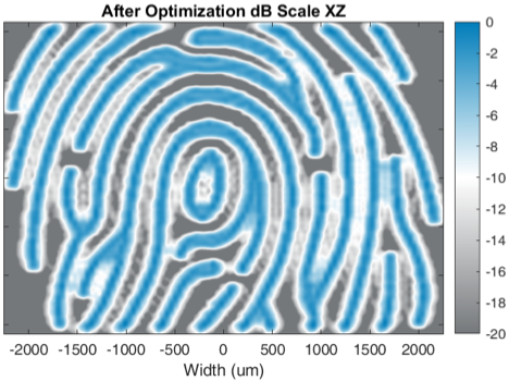
Without this large-scale simulation ability, sensor engineers would not be able to simulate a full model, leaving them with only analytics to determine the viability of their algorithms or whether their packaging, material and dimensional tolerances were optimal for performance and design objectives. As a result, the new sensor would have to be physically prototyped many times over to empirically resolve these design and manufacturing challenges—a process that would typically take months instead of hours in OnScale.
“When making sensors, you’re using a foundry partner, making silicon and creating processes to make them that take time to make sure they’re stable,” Harvey explains. “You lose money to develop these processes, and if the sensors don’t work, you have to start again.”
By using an HPC simulation platform, OnScale can deliver the answers before building physical prototypes, which saves time and costs, according to the white paper. The paper is meant to provide a real-world example to stave off the skepticism surrounding what’s possible with cloud-based simulation.
Check out this video to learn more about OnScale and how it is positioning its cloud CAE platform to help push breakthroughs in cost and performance for engineers designing mobile devices for 5G.

OnScale is the first Cloud Engineering Simulation platform. OnScale combines powerful multiphysics solver technology with the limitless compute power of cloud supercomputers. With OnScale, engineers can run massive numbers of full 3D multiphysics…

Structural Analysis with OnScale Solve™
In this webinar, we'll cover what's necessary to run a structural simulation in OnScale Solve, and how simulation on HPC in the cloud can accelerate this process for large design studies.
Beth Stackpole is a contributing editor to Digital Engineering. Send e-mail about this article to [email protected].
Follow DEJoin over 90,000 engineering professionals who get fresh engineering news as soon as it is published.


About Us · Contact Us · Editorial Team · Advertising · Privacy Policy · Subscriber Services · © 2026 Digital Engineering 24/7 · Peerless Media