Helping design and engineering professionals discover, evaluate and specify technologies and processes that shorten the design cycle and enable success.

May 2026 Special Focus: Artificial Intelligence in Design and Simulation
In this Special Focus Issue, learn about the latest developments in the integration of artificial intelligence into engineering workflows.

April 2026 Special Focus Issue: Generative Design
In this Special Focus Issue, Digital Engineering takes a look at how generative design solutions can be used across different types of design problems and with a variety of manufacturing approaches to accelerate design space exploration, and…
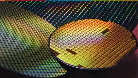
Cadence reports major advancements in chip design automation and IP, driven by its long relationship with TSMC to develop advanced design infrastructure, for artificial intelligence (AI) and high-performance computing (HPC) customer applications. Cadence and TSMC have collaborated on solutions from AI-driven electronic design automation (EDA) to 3D-ICs to IP and photonics, enabling advanced semiconductors, the company says.
Cadence and TSMC have worked on design infrastructure for advanced process nodes, including TSMC N3, N2 and A16. Cadence AI design flows for chip and 3D-IC are now available for TSMC’s advanced N3, N2 and A16 process technologies, as well as for new features in TSMC 3DFabric. Additionally, Cadence is collaborating with TSMC on EDA flow development for TSMC’s A14 process, with its first PDK to be released later this year. Also several new Cadence IP are now silicon-proven and available for TSMC N3P.
“Cadence and TSMC remain committed to speeding up and improving the design process for advanced silicon for our customers,” says Chin-Chi Teng, senior vice president and general manager of the Digital and Signoff Group at Cadence. “We’re helping designers develop the next generation of AI and HPC by supporting TSMC’s leading technologies with AI features, IP and beyond.”
“TSMC, together with our Open Innovation Platform (OIP) partners like Cadence, is addressing some of the most intricate challenges in semiconductor development to drive higher performance and energy efficiency in AI systems,” says Aveek Sarkar, director of the Ecosystem and Alliance Management Division at TSMC.
Cadence and TSMC have partnered on AI-driven design solutions for joint customers. TSMC has enabled Cadence JedAI Solution, Cadence Cerebrus Intelligent Chip Explorer’s AI-driven implementation technology and productivity features powered by Innovus+ AI Assistant within Cadence’s digital full flow. Additionally, TSMC has validated new AI-driven features, such as automated design rule check (DRC) violation fixing assistance.
The Cadence 3D-IC solutions provide comprehensive support for TSMC’s advanced packaging and die stacking configurations offered by 3DFabric. The latest innovations include automation features for bump connections, physical implementation and analysis for multiple chiplets and smart alignment marker insertion. The AI-driven application of Cadence’s Clarity 3D Solver and Sigrity X Platform with Optimality Intelligent System Explorer enables and automates the 3Dblox-based system-level SI/PI analysis and optimization.
Cadence IP enables AI infrastructure by accommodating the memory and interconnect bandwidth capacity of next-generation AI LLMs, agentic AI and other compute-heavy workloads. New Cadence IP on TSMC N3P process technology includes an HBM4 IP at N3P, high-speed memory interfaces like LPDDR6/5X at 14.4G and DDR5 12.8G MRDIMM Gen2 IP. Cadence also offers connectivity with PCI Express (PCIe) 7.0 IP—achieving a 128GT/s, 224G SerDes for AI infrastructure—and an eUSB2V2 and Universal Chiplet Interconnect (UCIe) 32G IP that support emerging AI PC and chiplet ecosystems.
Sources: Press materials received from the company and additional information gleaned from the company’s website.

Cadence is a leading EDA and Intelligent System Design provider delivering hardware, software, and IP for electronic design.
DE's editors contribute news and new product announcements to Digital Engineering. Press releases may be sent to them via [email protected].
Follow DEJoin over 90,000 engineering professionals who get fresh engineering news as soon as it is published.


About Us · Contact Us · Editorial Team · Advertising · Privacy Policy · Subscriber Services · © 2026 Digital Engineering 24/7 · Peerless Media