Helping design and engineering professionals discover, evaluate and specify technologies and processes that shorten the design cycle and enable success.
Alert!
Digital Engineering ceased publication on July 1, 2026. This website remains available as an archive of engineering content.
For inquiries or information, please email [email protected].

May 2026 Special Focus: Artificial Intelligence in Design and Simulation
In this Special Focus Issue, learn about the latest developments in the integration of artificial intelligence into engineering workflows.

Design & Simulation Software Guide 2025
In this Special Issue, Digital Engineering presents its second annual guide to design and simulation software vendors.
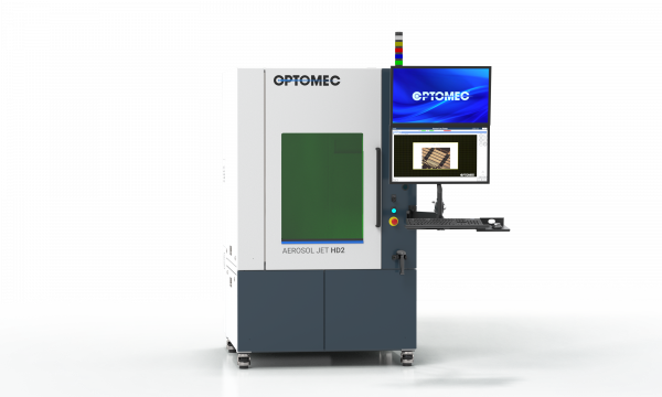
Optomec is announcing an advanced electronics packaging solution for miniaturization of mobile and wearable products. The Aerosol Jet HD2, uses Optomec’s Aerosol Jet 3D Electronics Printing solution to produce high-resolution circuitry, including an ability to dispense conformal 3D interconnects between die, chips, components and substrates. This interconnect approach offers improved performance at high frequencies, especially for 5G and mmWave applications.
Optomec’s Aerosol Jet HD2 targets the existing $4 Billion market for back-end semiconductor packaging and assembly equipment. The Aerosol Jet solution works by precision jetting or “printing” an extremely fine mist of nanoparticle-based inks onto a surface.
The HD2 can print features as narrow as 10 microns with placement accuracy under 5 microns. The nanoparticles are then sintered together, forming a solid metal conductor of copper, gold or silver. Insulating and adhesive materials can also be applied by the Aerosol Jet process with various integrated circuit packaging dielectric materials.
As a primary application, the Aerosol Jet HD2 can serve as a drop-in replacement for the method of connecting electrical components with wire bonds, which have some deficiencies. First, wire bonds require high impact mechanical contact with the IC, often producing scrap, especially with fragile, next-generation gallium-based chips. Second, wire bond loops require extra space within the package, making it harder for designers to create sleek, miniature devices to meet the demands of consumer electronics. Third, wire bonds can choke off the high-frequency mmWave signals required for 5G communications, automotive radar and many other emerging applications.
“The HD2 really changes the way designers think about IC packaging,” says Bryan Germann, aerosol jet product manager. “Not only can it reduce the size of the final electronics package, but it also out-performs wire bonding when it comes to high-frequency signals. Wire bonds simply produce a lot of inductance for RF applications above 40 GHz.”
The HD2 electronics printer also can be used to print transmission lines, sensors and antennas on various materials including common polymers, IC materials, FR4, glass, ceramic and metals. The HD2 was designed for high volume manufacturing and includes production-friendly software that guides operators through a simplified start-up process, ensuring QA compliance. The machine is also available with an in-line conveying option for automated part loading. It can process substrates or part trays up to 300-mm wide and is available with a rotate table for four-axis processing.
Sources: Press materials received from the company and additional information gleaned from the company’s website.

Optomec printers offer unique advantages over traditional approaches to 3D printing. Most industrial 3D Printers on the market today print plastic parts used as a visual mock-up for the real end-user part. In some cases, 3D Printers will deposit…
DE's editors contribute news and new product announcements to Digital Engineering. Press releases may be sent to them via [email protected].
Follow DEJoin over 90,000 engineering professionals who get fresh engineering news as soon as it is published.


About Us · Contact Us · Editorial Team · Advertising · Privacy Policy · Subscriber Services · © 2026 Digital Engineering 24/7 · Peerless Media