The Answer is in the Package
Latest News
September 1, 2016
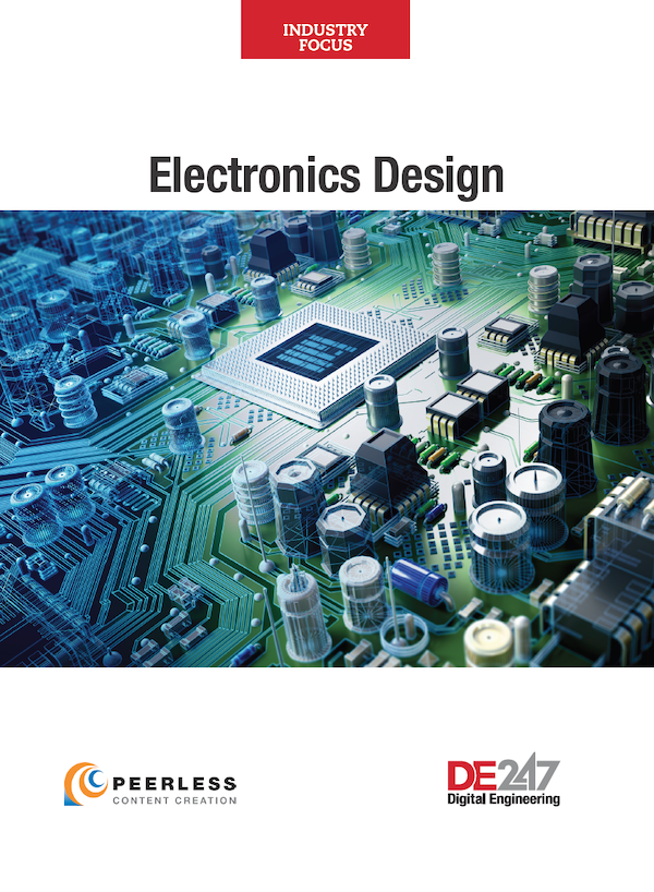
 It’s become increasingly difficult to distinguish between a chip, a board and a system. Design engineers are blurring the boundaries of each of these electronic components in attempts to meet shifting market demands.
To understand the forces driving this trend, you have to look at the proliferation of mobile devices and the emergence of the Internet of Things (IoT) and wearable devices. As these technologies gain traction, they place enormous pressure on design engineers to push the limits of form, function and energy efficiency. This translates into putting more sensors, memory and processing power into less space and supporting all of these functions with a miserly energy budget.
Unlike previous generations of engineers, today’s designers probably won’t find the answer to these dilemmas by reducing the size of electronic components. The sad truth is that the days of making smaller and smaller ICs (integrated circuits) are nearing the end. As a result, semiconductor manufacturers and device designers have turned to advanced packaging technologies to meet market expectations.
A New Era for Electronics
This new focus on packaging marks a major about-face for the electronics industry, and it promises to trigger significant changes in design processes. Up to this point, the semiconductor package has been an afterthought. Now the industry sees it as a key part of the design process and a critical factor in the effort to extend Moore’s Law.
Yole Développement published a report titled Status of the Advanced Packaging Industry 2015 supporting this view and saying that 2015 marked the beginning of a new era for the electronics industry. The report’s authors contend that companies will increasingly embrace advanced packaging to achieve greater integration, with the ultimate goal of reducing production costs and enhancing system performance.
One of the leading technologies in the advanced packaging arsenal is the system in package (SiP). This design approach enables the integration of heterogeneous, diverse and separately manufactured parts into a high-level assembly that bundles RF, processor, memory, sensing and power chips in a cohesive unit.
In a SiP, multiple bare die reside on a common substrate, which provides connectivity for all components on the die. The substrate and the components are then assembled in a single package. Using this approach, designers can incorporate a number of off-the-shelf die. This allows semiconductor providers to re-invent the device in the future by modifying or replacing individual die to deliver new functionality.
The SiP approach offers other advantages as well, such as smaller form factors, design flexibility and faster time to market. This architecture also opens the door for the integration of MEMS (micro-electro-mechanical systems) sensors on separate die, providing a way to accommodate the expanding sensor population brought on by the IoT while keeping footprints small.
Bringing Order from Chaos
Design engineers can reap SiP’s advantages using a variety of assembly techniques, including 2D, 2.5D and 3D ICs. While these options provide the designer with greater flexibility, they also introduce an element of chaos that has up until now precluded SiP’s entrance into high-volume markets. There are simply too many package types and process flows.
In response to this challenge, the semiconductor industry has begun work on establishing roadmaps for the integration of heterogeneous multi-die devices and systems. This move has the support of IEEE’s Components, Packaging and Manufacturing Technology Society (CPMT) and its Electron Devices Society.
As advanced packaging plays a more prominent role in the design process, engineers will face a raft of new challenges. The core issue lies in the fact that there are too many options and too little data to guide designers on what works best in terms of achieving consistent yield for economies of scale. Standards will help with this, but this metamorphosis will also require a more holistic view of the design process.
Decisions on how chips are packaged often affect other areas of the design in unexpected ways. For example: Even minor changes in the package can significantly alter the electrical or thermal characteristics of the system. As a result, collaboration at the system level becomes essential. Those who fail to adopt this approach will inevitably run into difficulties.
Subscribe to our FREE magazine, FREE email newsletters or both!
Latest News


