Helping design and engineering professionals discover, evaluate and specify technologies and processes that shorten the design cycle and enable success.
Alert!
Digital Engineering ceased publication on July 1, 2026. This website remains available as an archive of engineering content.
For inquiries or information, please email [email protected].


May 2026 Special Focus: Artificial Intelligence in Design and Simulation
In this Special Focus Issue, learn about the latest developments in the integration of artificial intelligence into engineering workflows.

April 2026 Special Focus Issue: Generative Design
In this Special Focus Issue, Digital Engineering takes a look at how generative design solutions can be used across different types of design problems and with a variety of manufacturing approaches to accelerate design space exploration, and…
If you look at electronic design automation (EDA), the entire chip design process is full of rule-of-thumb heuristics that have been built over decades. These rules are by no means perfect, but they usually get the job done. Until recently, they were the best guides available. That, however, is no longer the case. Machine learning (ML) has begun to carve out a niche in the semiconductor industry, enabling modeling and simulation to provide unprecedented levels of insight. As a result, engineers can expect greater accuracy and efficiency from design tools and a shift toward broader automation.
“EDA has many kinds of heuristics,” says Bryan Catanzaro, VP of applied deep learning research at NVIDIA. “Imagine that you’re doing placement and routing. You have to figure out where to put all the transistors and wires. You can’t actually get optimal placement because it’s such an enormous problem. But you kind of have some rules about how to minimize cost, and you may have algorithms that help you explore that space to a certain extent. So, the opportunity for machine learning in EDA is to replace some of those hand-coded heuristics with models that we learn from data. It turns out that the heuristics, while they work most of the time, aren’t as good as models learned from data.”
Perhaps the best way to see how ML can improve the design process is to look at the areas where today’s EDA tools fall short. Chip designers find themselves handicapped by the narrow visibility provided by current modeling and simulation technologies. Most of the shortcomings arise from the technologies’ limited ability to contend with the variability of physical attributes of system components and to sample and represent nonlinear surfaces and spaces. The situation is further compounded by inadequate information about physical interactions among components and correlations among input parameters.
 Machine learning stands poised to expand the capabilities of EDA, promising to deliver more accurate and efficient modeling and simulation. Image courtesy of ANSYS.
Because of these deficiencies, design engineers have difficulty modeling key design elements, and when they do, they cannot achieve the desired degree of accuracy. In addition, they are limited in what they can hope to do with simulation-based design optimization. At times, the issue isn’t that a facet cannot be modeled or simulated; it is that it cannot be done in a timely manner.
In the case of simulation, current technology simply cannot handle the large number of design variables involved. That said, behavioral models promise to address some of the flaws of current simulation technology. Unfortunately, the industry has yet to settle on a general, systematic method for generating these models.
One of EDA’s greatest shortcomings lies in its inability to glean insight from previous designs. Chipmakers have been designing chips, packages and systems for decades, and all of this information is available, hidden in databases that have never been tapped to facilitate new designs. “If we can only learn from these databases, the chances of errors in new designs can be minimized or eliminated,” says Madhavan Swaminathan, director of the Centre for Co-Design of Chip, Package, System, at the Georgia Institute of Technology. “We often rely on the experience of the designer, but why not learn from the experience of a machine that can sort through millions of data to determine possible patterns.”
Untapped resources is exactly what machine learning brings to the design process, and by turning mountains of raw data into valuable design insight, machine learning gives EDA a desperately needed shot in the arm.
 Chip designs are subject to process, voltage and temperature (PVT) variations, often modeled as a set of PVT corners. Process corners represent the extremes of the parameter variations within which a circuit must function correctly. Shown here is a fast PVT accuracy-aware model that uses a small number of simulation points, covering independent and interaction effects, to predict the remainder of the values. Image courtesy of Solido.
Until recently, even with the rules of thumb, chip design has been a relatively subjective process. After long hours of measuring physical parameters and running simulations, electronics engineers still fell into the trap of over-designing or under-designing the chips.
By adding ML to the EDA toolset, past experiences become training data that greatly expands the engineer’s modeling and simulation capabilities and provide greater transparency in the key issues determining the success of a design. Thus, the designer uses lessons of the past to glean the insight required to predict better solutions for new, similar problems. “To solve hard problems, you have to use large amounts of data, and so our current understanding of AI has evolved to support that,” says Catanzaro.
The experience of early adopters shows that applying ML to chip design not only improves the quality of designs but it also delivers significant business dividends. “Large design houses with abundant data in different design stages start to realize the potential of looking into the data to help them get the product to market earlier and save cost [at the] bottom line,” says Norman Chang, chief technologist at ANSYS.
Leveraging chipmakers’ bank of design info for training, ML uses algorithms to identify patterns to optimize design. The patterns map input attributes to the desired output feature or process outcome. This allows ML to create models to capture these patterns.
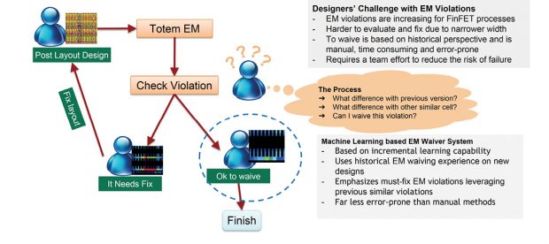 An ML-based electro-migration (EM) violation waiver system co-developed by NVIDIA and ANSYS uses historical EM waiving experience to provide a faster more accurate way of identifying must-fix EM violations. Image courtesy of NVIDIA/ANSYS Design Track paper at DAC 2017.
By using the insights gleaned from the training data, designers can efficiently model greater levels of complexity. This translates into models that accommodate physical attribute variables, nonlinear spaces and surfaces and complex interactions among components and subsystems—all without human intervention.
“Machine learning can take the data associated with the variability of physical attributes and build advanced machine learning models of this variability,” says Amit Gupta, president and CEO of Solido Design Automation. “These models can be high-dimensionality, nonlinear model discontinuities, along with high-order interactions.”
This approach has proven to outperform models created by humans using traditional techniques. “If you’re not using machine learning to understand model variability, what are you using?” asks Catanzaro. “You’re using a simpler model that a human built, and that’s not going to understand the complexities and the interdependence of the attributes of this physical system in the way that a model trained by data can. When humans build models they often assume independence of physical attributes in a way that isn’t actually justified. But machine learning models don’t need to make these assumptions because we’re not actually building them by hand. We’re learning from the data.”
Because of these advantages, ML-generated models provide better feedback to engineers, indicating if the design will deliver the desired performance at each step of the development process. Often, the process of designing a chip is very complicated, with many rules to learn and many ways to violate those rules. Having models that can help the engineer analyze the design and understand when a rule has been violated makes the development process more efficient. Machine learning can help engineers identify and interpret the problems that they have with their designs faster, enabling them to be more productive.
It’s important to remember that whenever you have simulation and modeling, the designer must strike a balance between fidelity and interactivity. During most chip design work, the engineer uses many different models, each of which is at a different point in the trade-off. “The thing that’s really interesting about machine learning is that it opens up new possibilities for us to augment this trade-off between different types of simulation with models that we learn from data,” says Catanzaro. “What that can help do is either make a model with a given level of interactivity more accurate, or alternatively, it can create a new model that’s very interactive—maybe not quite as accurate—but so interactive that designers can change the way they do their work.”
For example, let’s say you had a tool that was going to perform place and route on your design. What if you had a model that could predict the results before you actually create a prototype? It might take a day or a week to actually run that placement route, but if you had a model that could predict that for you, you might make different decisions. That’s an opportunity to change the way designers work, giving them a model that’s more interactive than the one they currently have.
Another benefit that ML brings to EDA is greater efficiency, which translates into shorter turnaround times and greater analysis flexibility and simulation coverage. Consider, for example, the ML-based electromigration (EM) violation waiver system co-developed by NVIDIA and ANSYS, which continuously learns to improve its analysis as it is trained with new design data.
In this application, gradual damage caused by on-chip EM can compromise the physical integrity of wires, impairing the system’s performance and reducing its lifetime. To mitigate the effects of EM, designers must be able to ensure that layouts can resist them. Unfortunately, traditional EDA tools have proven problematic.
“Manually analyzing the results generated by EDA tools to waive or fix any violations is a tedious, error-prone and time-consuming process,” says Chang. “By automating these manual procedures by aggregating key insights across different designs, using continuing and prior simulation data, a design team can speed up the tape-out process, optimize resources and significantly minimize the risk of overlooking must-fix violations that are prone to cause field failures.”
The same kind of efficiency can be seen in another application, where machine learning is used to support thermal design optimization for 3D ICs. Professor Swaminathan and his colleagues at the Georgia Institute of Technology performed 3D thermal simulation of a power delivery network, using the resulting thermal profile to perform circuit simulation to measure clock skew.
“A major problem with 3D ICs is thermal management, where trapped heat can create hot spots and thermal gradients across the IC, which in turn affect clock skew,” says Swaminathan. “Managing thermal gradients across the IC can be daunting since power densities change with time and several control parameters can affect it. An ML approach in such a scenario can be very useful since it can help augment multiphysics simulation, support the tuning of parameters while designing the system, and enable the functioning of a closed-loop control system for thermal management.”
The researchers had to run numerous simulations before they found a design that met the application’s requirements for clock skew. Using a statistical learning method called Bayesian optimization, the team reduced the number of simulations.
A third example shows how ML modeling and simulation can enable verification to cover operating parameters. Current verification approaches try to cover a spectrum of operating parameters or corners via explicit programming. Unfortunately, the number of corners continues to grow as device physics get more complicated due to shrinking device feature size and line widths.
“By applying machine learning, the important corners and their associated parameters can be learned or derived via an adaptive model, providing the widest possible coverage in a feasible timeframe,” says Shiv Sikand, executive VP and co-founder of IC Manage.
If ML has so much to offer EDA, why doesn’t it play a bigger role in semiconductor design? Some might say it’s still in its infancy, but that is not quite accurate. You have to go back 60 years to find its roots in chip design. Around 10 to 15 years ago, researchers did extensive work using artificial neural networks to model circuits. But nothing materialized from this research because the industry did not believe that there was a need for it.
“Chip design and EDA have not yet benefited as widely from machine learning because it has been possible to build chips and do EDA without those algorithms,” says Catanzaro. “There are a lot of really strong approaches to solving chip design problems that people developed without machine learning. So the bar is pretty high. To displace those approaches, you have to have something that is better.”
But, it appears that the industry has nearly reached the tipping point. Engineers recognize the value of the design data that resides in chipmakers’ databases. Designers increasingly have access to adequate computing resources. And the complexity of systems may have outstripped the capacity of current EDA tools.
With the need all but established, the big question is: Is there enough working knowledge of ML to capitalize on the technology? “Today the timing is just right due to the complexity of systems that we are building, but the know-how on the application of ML techniques for IC design is low within companies,” says Swaminathan. “Hence, industry is relying more and more on universities to help them with the development of new ML algorithms and for developing the next workforce. But companies are not willing to share data with the universities because most of the data is proprietary and confidential. Without data, ML cannot be advanced. Hence, we have a chicken-and-egg problem here that represents a major obstacle.”
Centre for Co-Design of Chip, Package, System, at the Georgia Institute of Technology
DE survey respondents’ impressions of AI and machine learning:
“Machines that can design machines will mean that they will become smarter than man. This could mean the end of mankind as we know it.”
“I think it will be able to learn how a person works and predict what they would do next to speed up design.”
“AI and ML are the future of design and manufacturing.”
“AI has great potential, but there is the ‘black box’ problem where the reason for the decision making cannot be totally known which may cause issues for defense, aerospace and medical applications.”
“Heavily dependent on input data available. Will advance more when IoT technologies allow for real-time data collection during processing.”
“I think that ‘machine understanding’ will be more useful than what is currently billed as ‘machine learning.’”
“The most significant innovation of our century. It will guide design, lower costs and introduce continuous production change.”

Tom Kevan is a freelance writer/editor specializing in engineering and communications technology. Contact him via [email protected].
Follow DEJoin over 90,000 engineering professionals who get fresh engineering news as soon as it is published.


About Us · Contact Us · Editorial Team · Advertising · Privacy Policy · Subscriber Services · © 2026 Digital Engineering 24/7 · Peerless Media