Helping design and engineering professionals discover, evaluate and specify technologies and processes that shorten the design cycle and enable success.
Alert!
Digital Engineering ceased publication on July 1, 2026. This website remains available as an archive of engineering content.
For inquiries or information, please email [email protected].
Digital Engineering April 2026
In the latest issue of Digital Engineering, we take a look at the latest innovations in design for additive manufacturing, including the use of natural language inputs, social media cosplayers, and AI integration. The issue also includes a feature…

January Special Focus Issue: Design for Additive
In this Special Focus Issue of Digital Engineering, learn about the latest advancements in design for additive manufacturing, including new software tools, additive in automotive, custom medical devices, and more.
The Lawrence Livermore National Laboratory (LLNL) has developed a way to use electrophoretic deposition (EPD) for AM in a new process the lab is calling light-directed electrophoretic deposition. EPD itself has been used for almost 100 years as a way of coating materials through deposition. As an example, new cars can be primed using EPD by moving a positively charged car body into a negatively charged dunk tank.

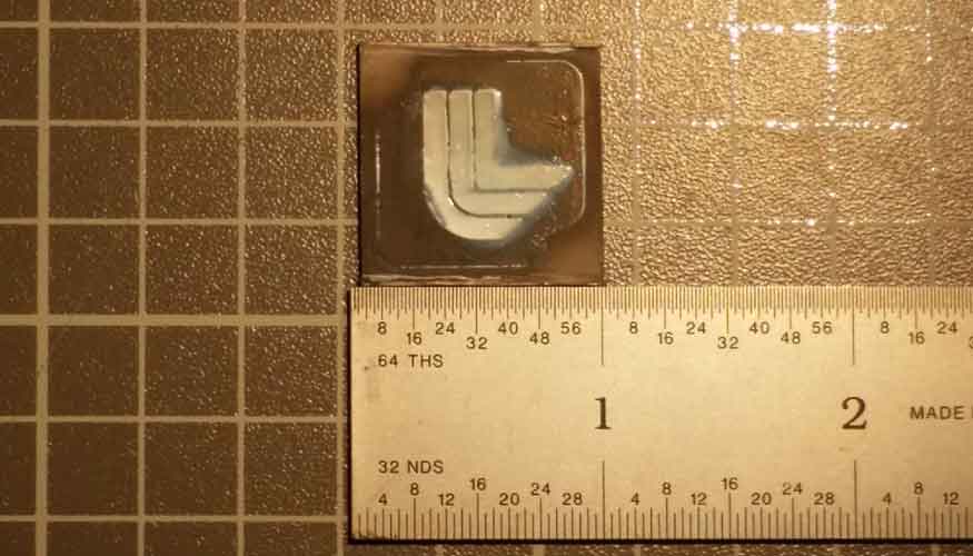
EPD can deposit materials on a wide variety of surfaces, including ceramics, metals, polymers, and even living cells, but has been limited to area dispersal patterns. LLNL’s project has discovered a method to force material buildup in specific areas, turning the old technology into an AM process. Researchers used photoconductive electrodes and DC electrical fields to direct the patterns of deposition, encouraging a layering effect in targeted areas where the light comes in contact with the photoconductor's surface.
From the press release:
Researchers used light-directed EPD to produce an alumina ceramic-tungsten nanoparticle composite. Initially, the tungsten nanoparticles were deposited across the photoconductive surface, then illuminated through a laser cut aluminum mask. A different shaped mask was then substituted along with the new material, to deposit the ceramic material. In the future, the aluminum masks will be replaced by a digitally projected mask, similar to those found in DLP televisions, for a completely automated deposition system.
The results of the research have been published in Advanced Materials in a paper named “Light-Directed Electrophoretic Deposition: A New Additive Manufacturing Technique for Arbitrarily Patterned 3D Composites.”
"We have presented a novel electrophoretic deposition technique based on using light to pattern materials on a photoconductive layer. This represents a large step in advancing electrophoretic deposition as a method of fabricating complex 3D patterned composites," said Andrew Pascall, research engineer and lead author.
Below you’ll find a video from LLNL extoling the virtues of AM.
Source: LLNL

John Newman is a Digital Engineering contributor who focuses on 3D printing. Contact him via [email protected] and read his posts on Rapid Ready Technology.
Follow DE


About Us · Contact Us · Editorial Team · Advertising · Privacy Policy · Subscriber Services · © 2026 Digital Engineering 24/7 · Peerless Media