Helping design and engineering professionals discover, evaluate and specify technologies and processes that shorten the design cycle and enable success.
Alert!
Digital Engineering ceased publication on July 1, 2026. This website remains available as an archive of engineering content.
For inquiries or information, please email [email protected].


Design & Simulation Software Guide 2025
In this Special Issue, Digital Engineering presents its second annual guide to design and simulation software vendors.

Design & Simulation Software Guide
In this Special Issue, Digital Engineering presents its inaugural guide to design and simulation software vendors, including listings for CAD, CAM, simulation, generative design, PLM, rendering and visualization, design for additive manufacturing,…
In their 2001 paper titled “Sub-50 nm P-Channel FinFET,” (published in IEEE Transactions on Electron Devices, Vol. 48, No. 5, May 2001), authors Huang, Lee, Kuo, Hisamoto, et al. observed “Scaling of device dimensions has been the primary factor driving improvements in integrated circuit (IC) performance and cost, which have led to the rapid growth of the semiconductor industry ... The double-gate MOSFET is considered the most attractive device to succeed the planar MOSFET ... The FinFET, a recently reported novel double-gate structure, consists of a channel formed in a vertical Si fin controlled by a self-aligned double-gate.”
Nearly two decades later, FinFET is no longer a novel technology but something “the industry is moving toward,” according to Semiconductor Engineering. (See FinFET in a Few Words, page 22.) The move from planar to 3D transistors also demands innovative thermal strategies.
“When the heat trapped in the FinFET’s 3D structure needs to escape, it usually finds the weakest thermal resistance as the point for exit. Just like how heat rises to the top floor in tall buildings, FinFET heat goes to the top, to the metal routing layer on the die. The accumulated heat on the die, which is called self-heating, along with the Joule heat from metal flow, can cause electromigration (EM) violation,” explains Jerry Zhao, product management director in the Digital & Signoff Group, Cadence.
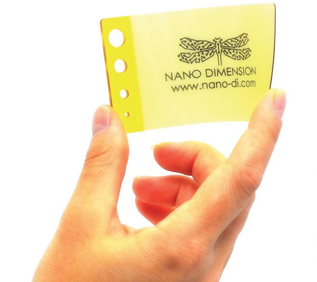 3D printers like Nano Dimension’s Dragonfly 2020 can print circuitry embedded inside objects, but currently state-of-the-art electrical and mechanical design tools don’t offer an easy way to design and analyze such objects. Image courtesy of Nano Dimension.
Depending on how the affected IC is deployed, the outcome of EM violation could be a minor inconvenience (a failed smartphone) or a major disaster (a failed self-navigating automobile). The key to EM prevention rests with figuring out the right kind of simulations to run.
Typical IoT devices reflect their multitasking users’ behavior. A smartphone is not running one operation at a time. It’s managing the command streams of several apps simultaneously. That calls for rule-based power-jostling among the internal components, known as “throttling.”
“You put an upper-bound limit of temperature on the device,” explains CT Kao, software engineering director in the Custom IC & PCB Group, Cadence. “If it reaches that upper-bound, the device has to play with throttling—the allocation of the power to components.” Improper throttling—getting the power allocation strategy wrong—means burned chips, device failures and potentially lawsuits and public relations disasters for the brand.
One of the keys to figuring out throttling is the use of simulation to identify hot spots—regions in the device that will heat up to an unacceptable level during certain combinations of operations. “Most people do multiple things in a transient fashion, so things are going on and off frequently,” says Kao.“You have multiple chips, multiple power schemes. For example, in one scheme, one chip is on and two chips are off. You have many such combinations, so each configuration needs to be simulated.”
To understand the heat accumulation, it’s not enough to simulate a snapshot in time. The engineers must instead simulate a power scheme in operation for a reasonable span of time to be able to see where and how hot spots emerge. These so-called transient simulations are costly, both in time and money.
“If a designer wants to study one time step in detailed resolution, say, it takes about an hour. If your overall interest is a 10-second event, you need to be looking at [time slices of] 0.1- or 0.01-second intervals. From a simulation point of view, each time step is a new simulation run essentially, so if you have a simulation with a 1,000 time steps, you’re basically running the same simulation a thousand times. And if you have 100 power schemes to look at, you’ll effectively run out of time,” Kao adds.
It’s not that it’s impossible to simulate all 100 power schemes. But doing that would push the product design cycle so far behind, or add so much computation cost in server usage, that it becomes an impractical solution. That forces the designers to make difficult choices, in what to simulate—and at what level of detail.
There’s no one-size-fits-all solution. Or rather, there’s no single solution that can tackle the problems of different sizes. That’s one of the challenges that electronics design software makers like Cadence are working to overcome.
In the now industry-preferred FinFET transistors, at the substrate level, objects are measured in nanoscale, indiscernible to the naked eye. At the board level, objects are solid, discernible and measurable using traditional metrology tools. The heat generated in the FinFET travels through the integrated circuits (ICs) and the printed circuit board PCB. But what kind of partial differential equations can effectively be applied to solve the math governing the thermal behaviors observable at both the substrate level, the board level and the product level?
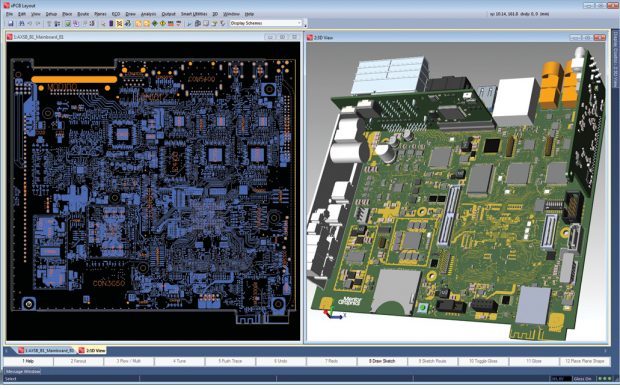 The convergence of ECAD and MCAD results in tools that allow the two disciplines to work closely together in a single environment. Shown here is Mentor Graphics Xpedition, with 3D visualization and validation within the PCB/ECAD environment. Image courtesy of Mentor Graphics.
“You don’t want to solve heat problems for a large solid object, like a watch, using the simulation formulation aimed for solving microscopic silicon-level behaviors,” says Kao. A single tool that can simulate the entire device at different resolution levels remains elusive to the industry, he notes.
It comes down to resolution, or mesh size, as simulation software users call it. In subdividing the geometry into tiny sections for analysis, applying nanoscale meshes to larger objects would unnecessarily increase the complexity of the job and the computation time. By the same token, meshing the geometry at the product level may not be fine-grained enough to identify heat build-ups at the transistor level. Engineers have to decide, based on experience and intuition, the critical question: What level of accuracy is sufficient for a given product or design?
“The designer needs to know the hot spots that appear at a specific time. If the resolution of the tool cannot provide that within the critical power cycle, the designer won’t catch that,” says Kao.
For the computation bottleneck, ubiquitous access to high-performance computing (HPC) via affordable private clusters and on-demand cloud service provides an outlet. But the accuracy of the results in HPC remains a concern, notes Zhao.
SPICE simulation (which stands for an open source Simulation Program with Integrated Circuit Emphasis) remains “the mother of all simulation,” says Zhao. It’s possible to run such simulation jobs on multi-core, multi-node clusters to speed up the job, but you need a good parallel solving technology, he adds.
“[HPC-based simulation] is like a military march or a band march. The last row needs to keep up with the first row. Otherwise, the pattern falls apart,” says Zhao. “You need something like a brain that controls the movements.”
Zhao and his colleagues continue to develop and refine what they call “the matrix-solving technology,” a feature in the software that ensures the results are the same whether the job is executed on a single machine with multiple cores or across a network with dozens of nodes and hundreds of cores. “This technology is unique to us. It can take advantage of multiple cores in the cloud and artificial intelligence (AI),” he says.
Cadence offers 3D IC design and analysis tools, PCB design and analysis tools, and system-level design and verification tools. “We have unified solution at the die level, board level and package level,” says Zhao.
The IoT trends favor thin, light, form-fitting devices with aesthetically interesting surfaces over the manufacturing-friendly oval, rectangular and cylindrical products. This has resulted in the use of flexible PCBs, dubbed Flex Rigid boards. Many of them were incorporated into the flip phones that now seem quaint. Because of their bendable, flexible, fabric-like connectors, they can fit into tighter, smaller spaces that a rigid board cannot.
“Flex Rigid boards have been a common feature for a long time, but it’s increasing in adoption in smaller factors,” says Dave Wiens, business development manager for Mentor Graphics’ board division. “What’s less common are 100% or 75% flexible boards—that means, instead of the board being mostly rigid with some flexibility, it’s mostly flexible. That’s when you’re dealing with printed electronics and shaved silicon die so the silicon can flex along with the structure.”
3D printing vendors like Nano Dimension further test the industry with the ability to print objects with embedded conductive materials, effectively making it impossible to differentiate the object and the circuitry within.
“These new designs represent structures that we’re not used to seeing—PCBs that look like a round orb, or any possible shape you might think of,” observes Wiens. “People who are looking to push the limits of 3D printing won’t print box-shaped objects. They’ll print shapes that are much more unique.”
“Additive manufacturing of PCBs is at this stage primarily a rapid prototyping tool. The time from concept to testing can be shortened dramatically and the cost, at prototype volumes, can be reduced significantly also,” explains Simon Fried, president of Nano Dimension.
But it may not remain so for long. Customized 3D-printed PCBs are an ideal solution to the tight-fitting IoT devices. And the use of 3D printing for mass production is no longer a pipe dream; it’s proven to be feasible for the automotive industry, medical device industry and others.
As always, invention in one space creates a new need in another. Such a cycle has already seemingly begun in ECAD. “Now, you may have a piece of flexible electronics that can bend and stretch, like a Band-aid on a wound,” notes Wiens. “That kind of electronics moves in various directions that their predecessors haven’t. For design and analysis, that represents a challenge: How do you design them correctly? How do you analyze them?”
“Current state-of-the-art ECAD packages do not offer a solution to design, simulate or validate free-form geometry circuits. Nevertheless, the worlds of ECAD (electronics CAD) and MCAD (mechanical CAD) are converging,” says Fried.
In March 2017, Mentor Graphics was acquired by the manufacturing titan Siemens and folded into the Siemens PLM Software division. SOLIDWORKS, a division of Dassault Systèmes, struck up a partnership with ECAD developer Altium, resulting in CAD-friendly PCB design solution. Two years ago, Autodesk acquired EAGLE, which develops the PCB design software. The outcome is Autodesk EAGLE, a free download available for hobbyists and makers.
“It’s fair to assume that integration of ECAD and MCAD considerations into a single tool is inevitable. This is not yet the case, however,” says Fried. “This is why Nano Dimension has developed a convenient plug-in to SOLIDWORKS in order to facilitate freeform circuit and part design. This allows you to design items such as coils, antennas and new solutions to bracketing and harnessing.”

Kenneth Wong is Digital Engineering's resident blogger and senior editor. Email him at [email protected] or share your thoughts or suggestions at digitaleng.news/facebook.
Follow DE


About Us · Contact Us · Editorial Team · Advertising · Privacy Policy · Subscriber Services · © 2026 Digital Engineering 24/7 · Peerless Media